

Silicon refining process
a technology of silicon refining and process, which is applied in the direction of silicon compounds, chemistry apparatus and processes, silicates, etc., can solve the problems of increasing the cost and economic viability of solar cells, and the silicon required for a solar cell is more expensive than the required, so as to reduce the susceptibility of the nation's generation capacity, reduce the cost of manufacturing a solar cell, and change the way a large portion of electrical power is
- Summary
- Abstract
- Description
- Claims
- Application Information
AI Technical Summary
Benefits of technology
Problems solved by technology
Method used
Image

Examples
example 1
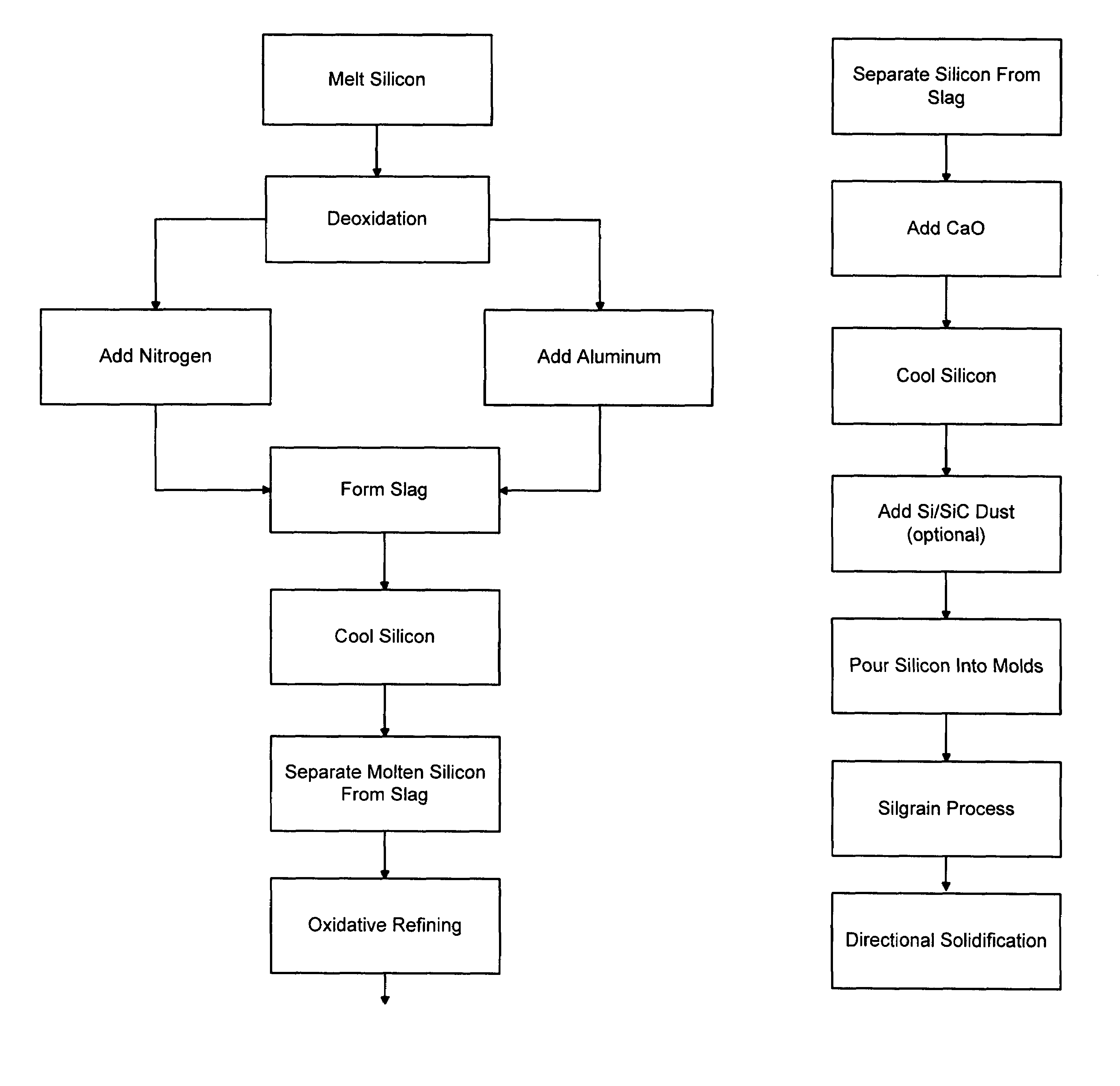
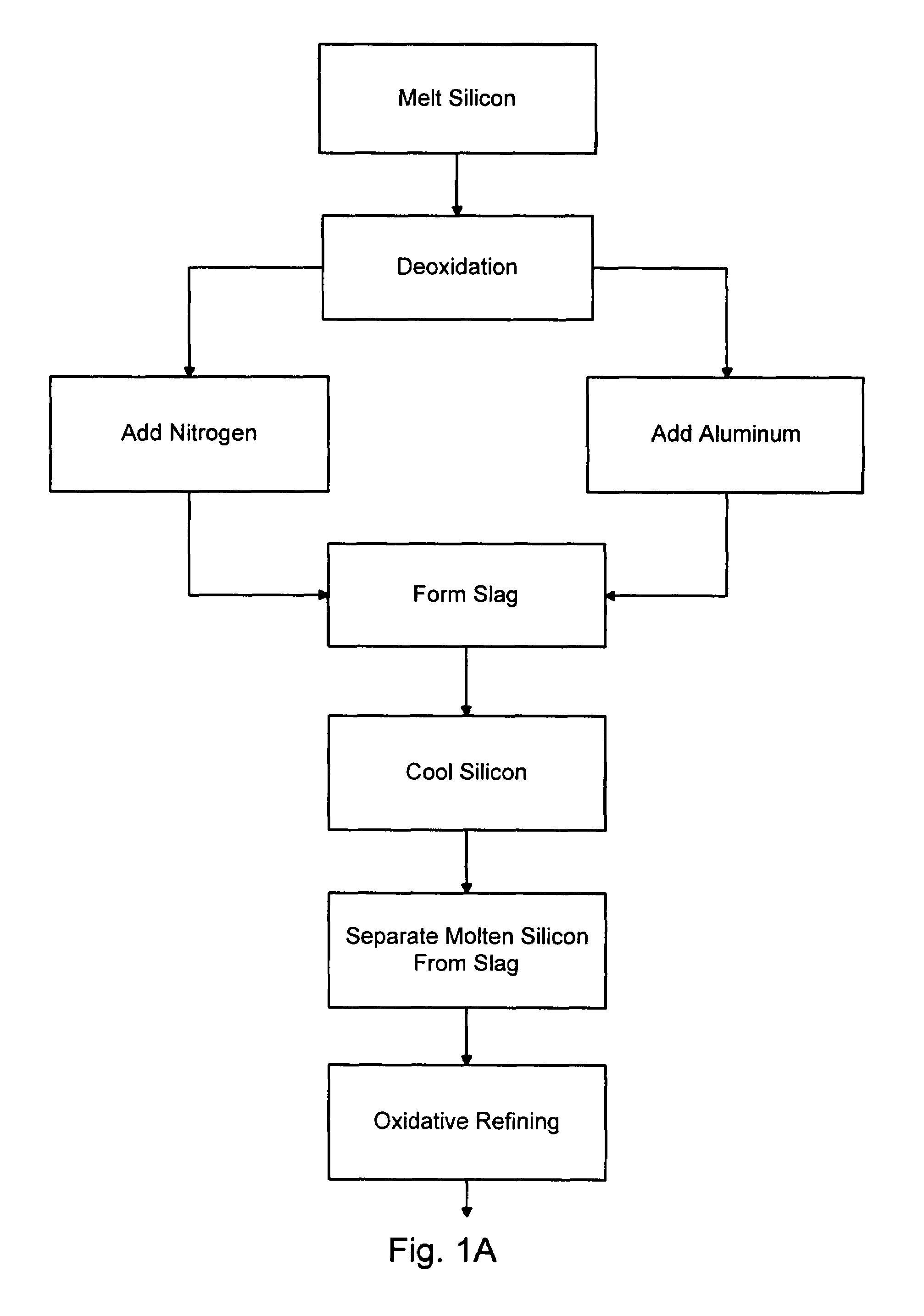
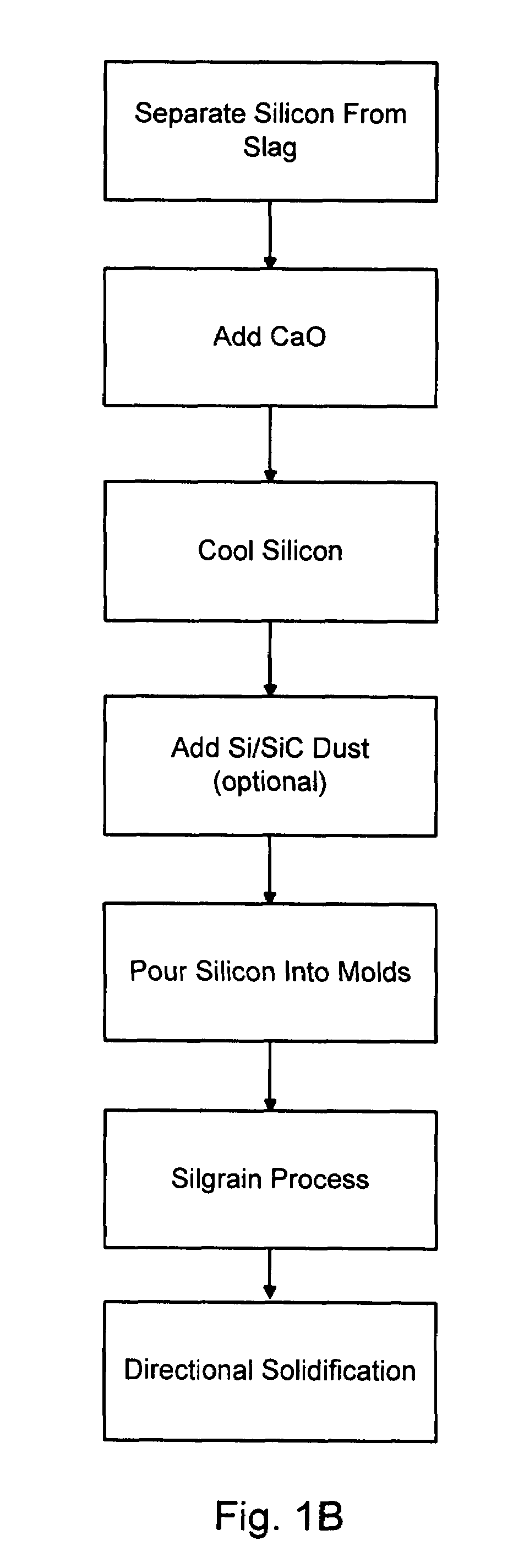
[0118]Example 1 contains a description of a typical process according to the invention which uses a slag and two vessels for deoxidation, nitriding and refining for boron and phosphorus, oxidative refining and SiC settling.
[0119]1. Metallurgical-grade silicon is charged to the cold crucible in the vacuum chamber. Any combination of Al2O3, CaO, MgO, Al, Ca, or Mg is included in the charge to achieve the desired level of
[0120]a. Al dissolved in the silicon for phosphorus refining.
[0121]b. Al dissolved in the silicon for AlN formation during and after nitriding. AlN dissolves in the slag.
[0122]c. Al, Ca, and Mg dissolved in the silicon to maintain a highly reducing condition during boron and phosphorus refining.
[0123]2. The chamber is sealed, then evacuated with a mechanical pump to 0.01 bar, and then back filled with purified N2 to a pressure of 1 bar or higher. This process may be repeated several times to effectively remove any residual air remaining in the chamber. The N2 entering ...
example 2
[0143]Example 2 contains a description of a typical process according to the invention using a solid discard phase. Deoxidation and nitriding are the same as described in Example 1 with some slight modifications.
[0144]Refining for boron and phosphorus takes place in a separate vessel. The melt is cooled to between 1700 K and 1880 K and then passed through a bed of particulate consisting of the βss (solid discard phase) to remove boron and phosphorus. The particulate is prepared in advance and is used in a near continuous process after which the particulate is removed and replaced with new particulate. The solid phase consists of a solid solution formed from Si3N4, Al2O3, AlN, MgO, and CaO. The solids are pieces from 2 mm to 10 mm in diameter. The bed is structured, with respect to composition, by having strata so as to remove boron and phosphorus separately, but with the optimum composition for refining of the silicon with respect to the bed material, so as to achieve the greatest e...
PUM
| Property | Measurement | Unit |
|---|---|---|
| temperature | aaaaa | aaaaa |
| temperature | aaaaa | aaaaa |
| temperature | aaaaa | aaaaa |
Abstract
Description
Claims
Application Information