Amplitude regulated crystal oscillator
- Summary
- Abstract
- Description
- Claims
- Application Information
AI Technical Summary
Benefits of technology
Problems solved by technology
Method used
Image

Examples
Embodiment Construction
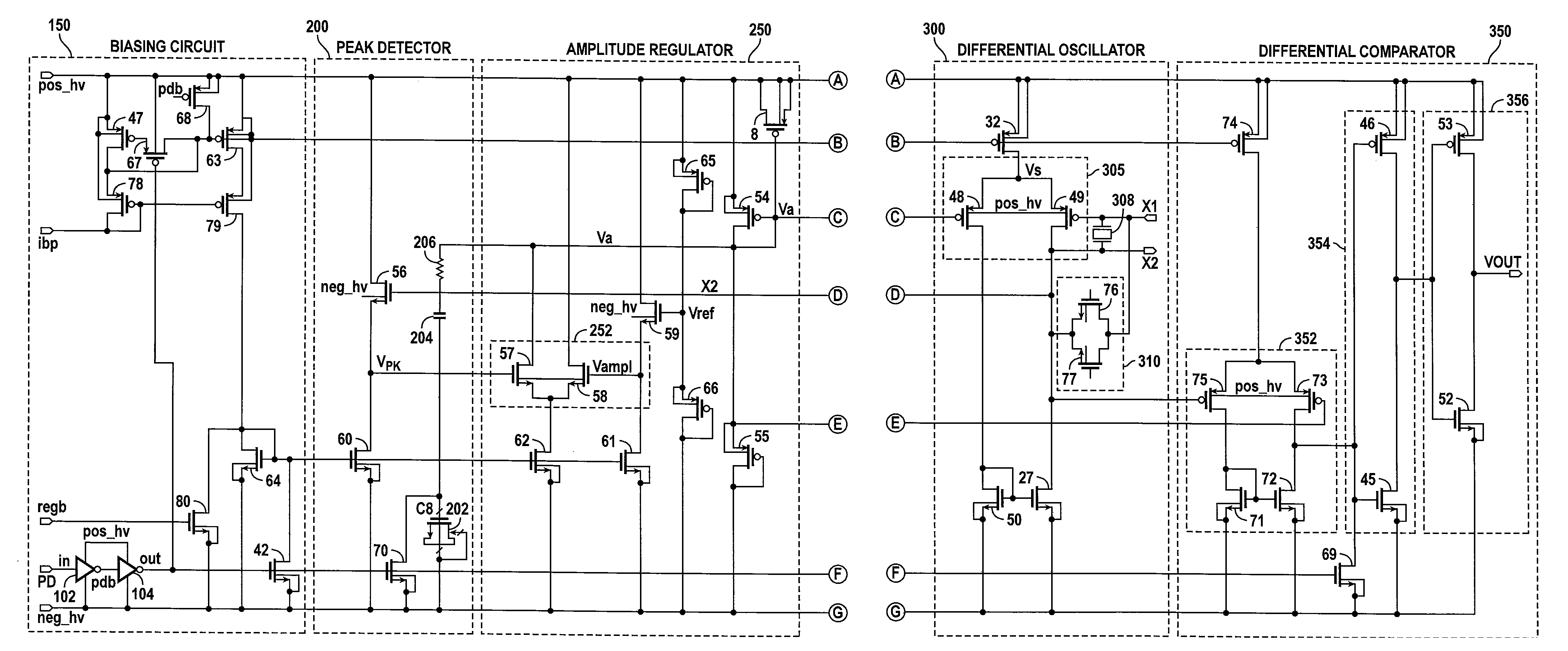
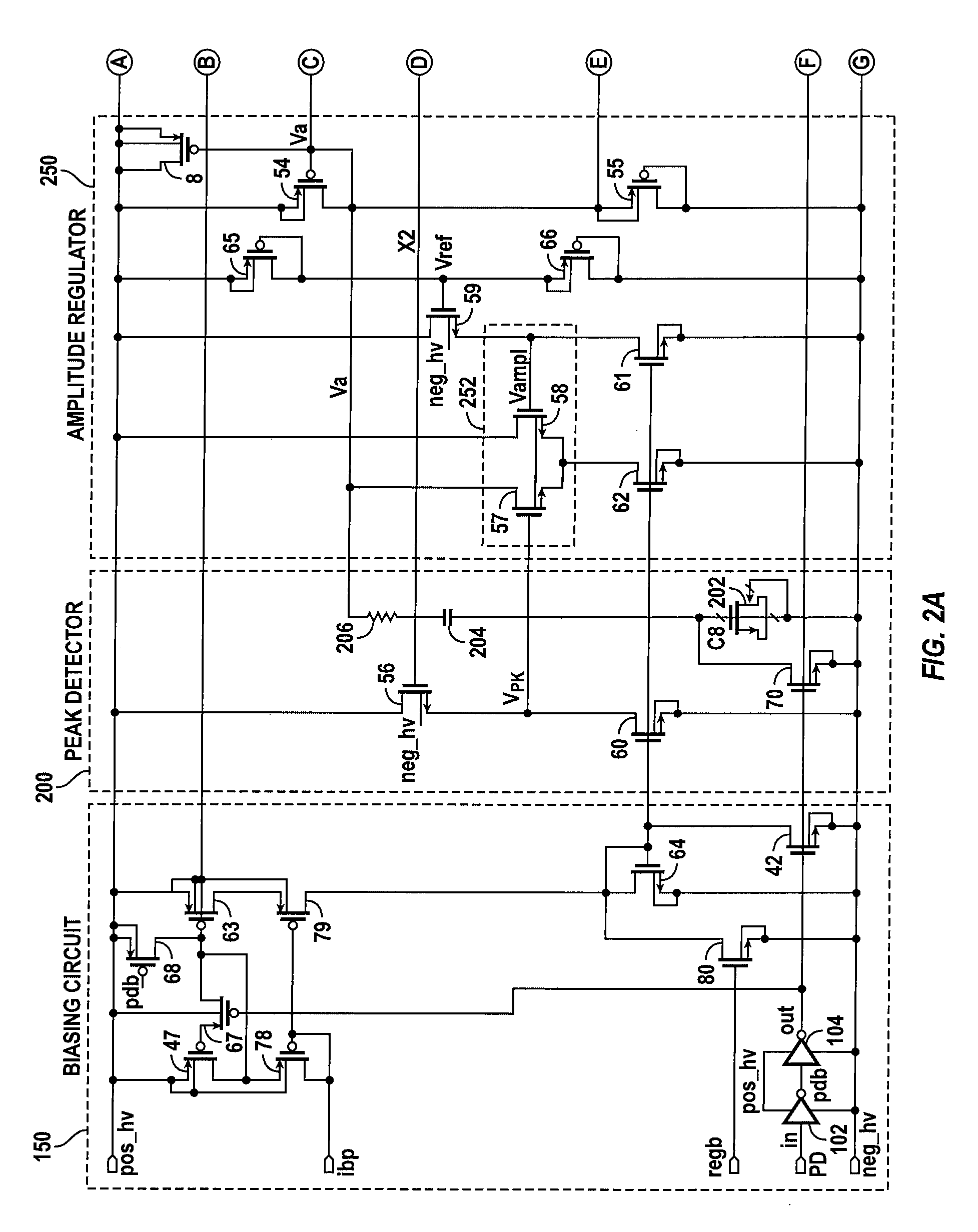
[0014]FIGS. 2A and 2B, collectively forming FIG. 2, are transistor schematic diagrams of an oscillator 100, in accordance with one embodiment of the present invention. Oscillator 100 is shown as including a biasing circuit 150, a peak detector 200, an amplitude regulator 250, a differential oscillator 300, and a differential comparator 350, in accordance with one embodiment of the present invention.
[0015]Transistors 47, 78, 63 and 79 of biasing circuit 150 form a cascode current mirror. Signal PD is applied to inverter 102 whose output signal PDB is applied to inverter 104. Signal PDB is applied to the gate terminal of PMOS transistor 68. The output signal of inverter 104 is applied to the gate terminal of transistor 67. Transistors 67 and 68 are used to power down biasing circuit 150, which in turn, turns off oscillator 100. Transistor 60 of peak detector 200 and transistors 61 and 62 of amplitude regulator250 are current source transistors biased using diode-connected transistor c...
PUM
 Abstract
Description
Claims
Application Information
 - R&D Engineer
- R&D Manager
- IP Professional
- Industry Leading Data Capabilities
- Powerful AI technology
- Patent DNA Extraction
Browse by: Latest US Patents, China's latest patents, Technical Efficacy Thesaurus, Application Domain, Technology Topic.
© 2024 PatSnap. All rights reserved.Legal|Privacy policy|Modern Slavery Act Transparency Statement|Sitemap