
Low dielectric constant group II-VI insulator

a dielectric constant and group ii-vi technology, applied in the direction of crystal growth process, sulfur compound, semiconductor laser, etc., can solve the problems of crosstalk noise, resistance-capacitance delay (rc delay), and limiting factors for ultra-large-scale integration of integrated circuits

Inactive Publication Date: 2010-04-06
ZENO MATERIALS LLC
View PDF29 Cites 18 Cited by
  • Summary
  • Abstract
  • Description
  • Claims
  • Application Information

AI Technical Summary

Problems solved by technology

The semiconductor industry is approaching a point at which conventional silicon dioxide dielectrics are inadequate for the function of insulating metal interconnects as the scale of integration and device speed increases.
As integrated circuit (IC) dimensions continue to decrease, resistance-capacitance delay (RC delay), crosstalk noise, and power dissipation of the interconnect structure become limiting factors for ultra-large-scale integration of integrated circuits.
It typically has its upper most energy band completely empty which results in extremely low conductivity.
P-type zinc oxide semiconductor materials are theoretically possible, but have been difficult to prepare.
Their stability has been questioned and instability has been observed.
Some of the more-stable p-type zinc oxide materials reported in the literature are prepared using complex and expensive fabrication processes, such as molecular beam epitaxy.
No commercially viable p-type zinc oxide semiconductor materials are currently known.

Method used


Image

  • Low dielectric constant group II-VI insulator

Examples


example 1

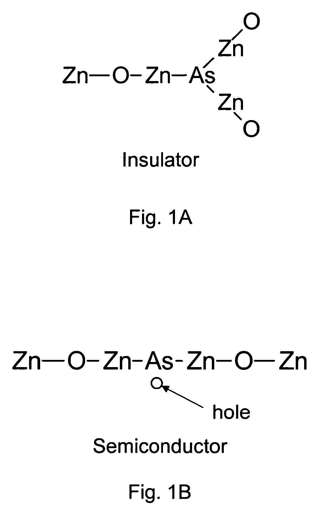
[0023]A low dielectric zinc oxide insulator material is fabricated by obtaining zinc oxide doped with arsenic at a dopant concentration of about ¼ mole %. The arsenic-doped zinc oxide possesses p-type semiconductor properties. The arsenic-doped zinc oxide is heated to a temperature greater than about 450° C. for a time period of about 10 minutes. The resulting arsenic-doped zinc oxide has been converted to an insulator and has a low dielectric constant.

example 2

[0024]A low dielectric zinc oxide insulator material is fabricated by obtaining zinc oxide doped with arsenic at a dopant concentration of at least 1018 atoms / cm3. The arsenic-doped zinc oxide possesses p-type semiconductor properties. The arsenic-doped zinc oxide is heated to a temperature greater than about 450° C. for a time period of about 10 minutes. The resulting arsenic-doped zinc oxide has been converted to an insulator and has a low dielectric constant.

example 3

[0025]A low dielectric zinc oxide insulator material is fabricated by obtaining zinc oxide doped with antimony at a dopant concentration of at least 1018 atoms / cm3. The antimony-doped zinc oxide possesses p-type semiconductor properties. The antimony-doped zinc oxide is heated to a temperature greater than about 650° C. for a time period of about 10 minutes. The resulting antimony-doped zinc oxide has been converted to an insulator and has a low dielectric constant.


PUM

PropertyMeasurementUnit
resistivityaaaaaaaaaa
temperatureaaaaaaaaaa

Abstract

Low dielectric constant group II-VI compounds, such as zinc oxide, and fabrication methods are disclosed. Low dielectric constant insulator materials are fabricated by doping zinc oxide with at least one mole % p-type dopant ion. Low dielectric constant zinc oxide insulator materials are fabricated by doping zinc oxide with silicon having a concentration of at least 1017 atoms / cm3. Low dielectric zinc oxide insulator materials are fabricated by doping zinc oxide with a dopant ion having a concentration of at least about 1018 atoms / cm3, followed by heating to a temperature which converts the zinc oxide to an insulator. The temperature varies depending upon the choice of dopant. For arsenic, the temperature is at least about 450° C.; for antimony, the temperature is at least about 650° C. The dielectric constant of zinc oxide semiconductor is lowered by doping zinc oxide with a dopant ion at a concentration at least about 1018 to about 1019 atoms / cm3.

Description

CROSS REFERENCE TO RELATED APPLICATION[0001]This application claims the benefit of U.S. Provisional Application No. 60 / 580,454, filed Jun. 17, 2004, which application is incorporated by reference.BACKGROUND OF THE INVENTION[0002]The present invention provides low dielectric constant zinc oxide semiconductors, low dielectric constant zinc oxide insulators, and to fabrication methods thereof.[0003]Since the introduction of the transistor, the semiconductor industry has seen an unprecedented rate of change in manufacturing productivity and device performance. The semiconductor industry is approaching a point at which conventional silicon dioxide dielectrics are inadequate for the function of insulating metal interconnects as the scale of integration and device speed increases. As integrated circuit (IC) dimensions continue to decrease, resistance-capacitance delay (RC delay), crosstalk noise, and power dissipation of the interconnect structure become limiting factors for ultra-large-sc...

Claims


Application Information

Patent Timeline
Patent Type & Authority Patents(United States)
IPC IPC(8): H01L21/00C01G9/02H01L21/28H01L21/31H01L21/3115H01L21/316H01L21/363H01L21/365H01L21/469H01L23/58H01L27/15H01L29/225H01L29/26H01L31/0296H01L31/0328H01L31/12H01L33/28H01S5/30H01S5/327H01S5/347
CPCB82Y20/00H01L21/02579C30B25/02C30B29/16C30B29/48H01L21/316H01L23/5329H01L29/225H01L31/02963H01L33/025H01L33/28H01L33/285H01L21/02551H01L21/02554H01L21/02565H01L21/02568C01G9/02C01P2006/40H01L21/3115H01S5/305H01S5/3054H01S5/327H01S5/347H01L2924/0002H01L21/02107H01L2924/00
Inventor BURGENER, II, ROBERT H.FELIX, ROGER L.RENLUND, GARY M.
Owner ZENO MATERIALS LLC
Learn More