Solid state imaging device and manufacturing method thereof

a solid-state imaging and manufacturing method technology, applied in solid-state devices, color televisions, television systems, etc., can solve the problems of attracting foreign matter to the lens surface, difficult to remove foreign matter once it is adsorption, and small bumps, so as to prevent static charge buildup on the micro-lens surface, prevent quality loss and yield loss, and prevent static charge buildup

Inactive Publication Date: 2010-04-06
FUJIFILM CORP
View PDF5 Cites 0 Cited by
  • Summary
  • Abstract
  • Description
  • Claims
  • Application Information

AI Technical Summary

Benefits of technology

[0005]In view of the foregoing, an object of the present invention is to provide a solid state imaging device, and a manufacturing method thereof, capable of preventing static charge buildup on surfaces of micro-lenses without changing an optical characteristic of these micro-lenses.
[0011]According to the present invention, the micro-lenses are formed directly on the transparent first conductive film, and the static charges on the surface of each micro-lens are discharged to the first conductive film. It is therefore possible to prevent static charge buildup on the micro-lenses without changing the optical characteristic (shape) of the micro-lens. This leads to prevent quality loss and yield loss of the solid state imaging devices due to the optical characteristic change in the micro-lenses or adsorption of foreign matter to the micro-lenses.
[0012]When each micro-lens is covered with the second conductive film, the static charges on the micro-lens surface are certainly discharged to the first conductive film, and the static charge buildup on the micro-lens surface is prevented more certainly.
[0013]Since the first conductive film is connected to a ground, the static charges on the micro-lens surface can be discharged to a ground (GND) through the first conductive film. The static charge buildup on the micro-lens surface is therefore prevented still more certainly.
[0014]In the manufacturing method of the solid state imaging device according to the present invention, the resin layer and the resist pattern are formed consecutively on the first conductive film, and then applied to the overall-etching (etch-back) process with using the resist pattern as a mask so as to form the micro-lenses. The micro-lenses are formed directly on the first conductive film in this manner, and the static charge buildup on the micro-lens surface is therefore prevented. Additionally, it is possible to make clearances between the micro-lenses, and to adjust these clearances to a desired size.
[0015]Since the resist and the resin layer have the same etching rate, the resin layer is etched into the exact shape of the resist pattern. Accordingly, the micro-lens of a desired shape is easily formed.

Problems solved by technology

Therefore, static charges tend to build up on a surface of the micro-lens, attracting foreign matter to the lens surface.
Since a top surface of the solid state imaging device has bumps standing out in the shape of the micro-lenses, it is difficult to remove the foreign matter once it is adsorbed.
Also, the bumps get smaller as pixels become smaller, and removal of the foreign matter will be more difficult.
However, when introduced to cover the micro-lens as described above, this conductive film may vary in thickness and possibly changes the shape of the micro-lens.

Method used


Image

  • Solid state imaging device and manufacturing method thereof
  • Solid state imaging device and manufacturing method thereof
  • Solid state imaging device and manufacturing method thereof

Examples


Embodiment Construction

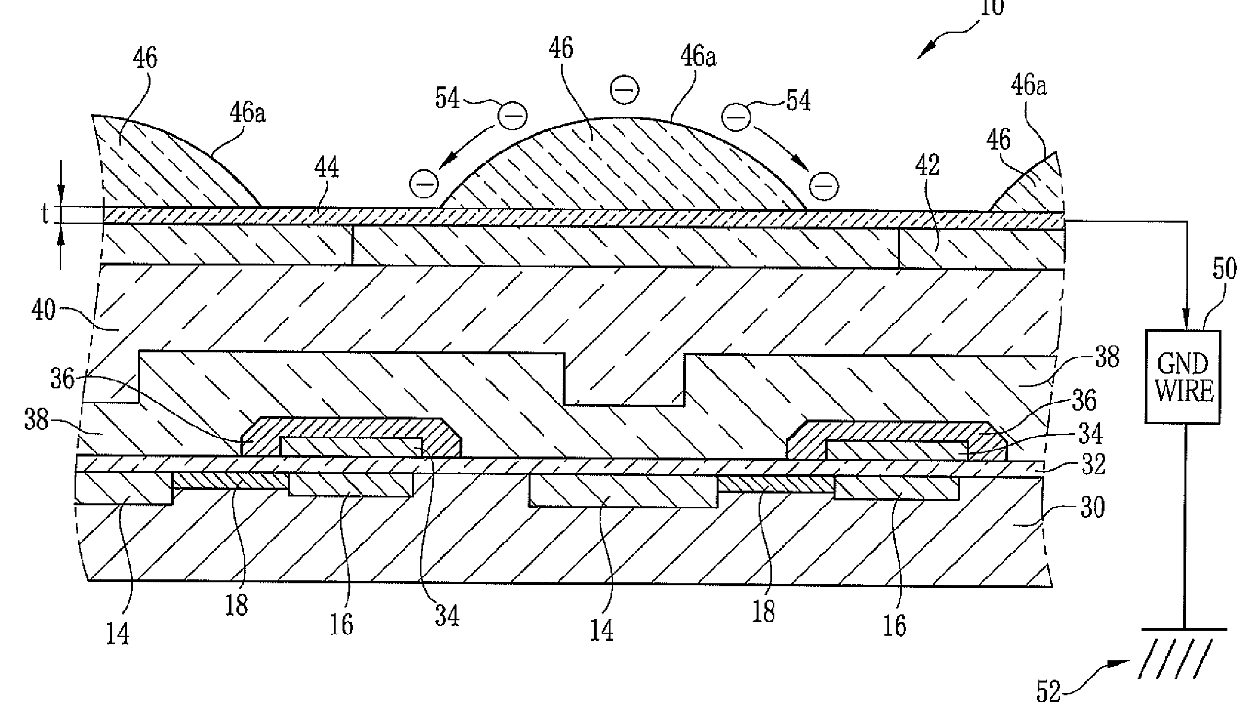
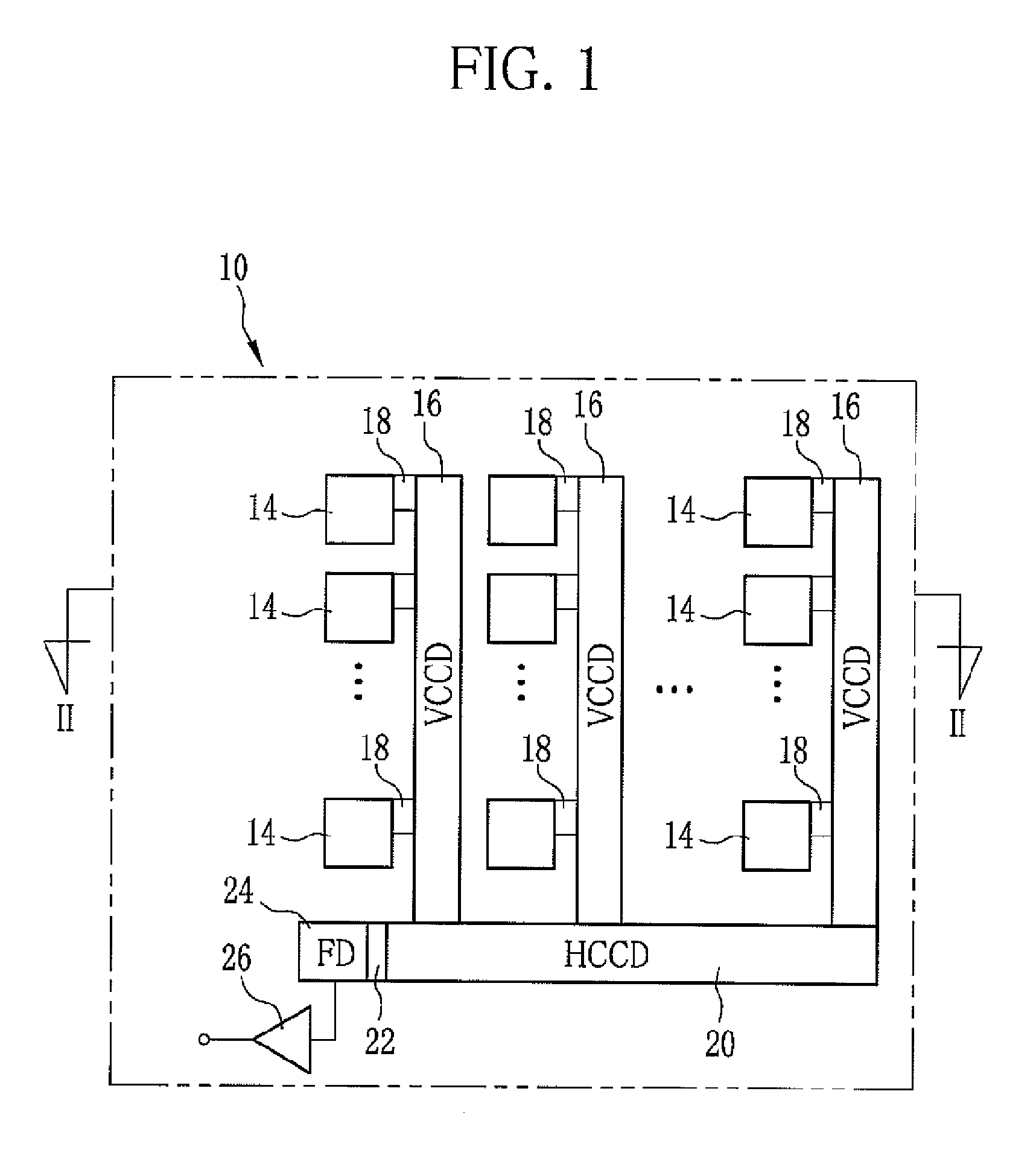
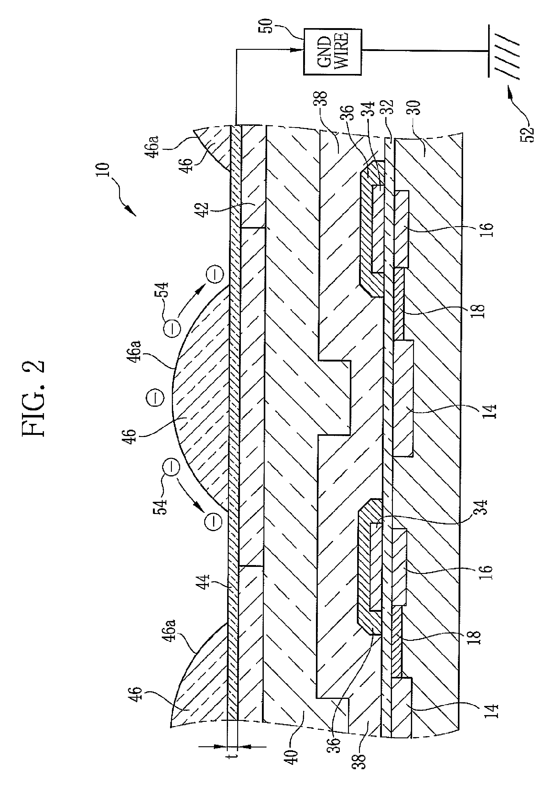
[0028]Referring to FIG. 1, a solid state imaging device 10 is an interline transfer CCD which includes plural photodiodes (light receiving elements) 14 in two dimensional matrix arrangement, vertical transfer CCDs (VCCDs) 16 along each column of the photodiodes 14, transfer gates (TG) 18 connecting each photodiode 14 to the VCCD 16, a horizontal transfer CCD (HCCD) 20 connected to output terminals of all the VCCDs 16, an output gate (OG) 22 and a floating diffusion (FD) 24 at an output terminal of the HCCD 20, and a source-follower amplifier circuit 26 connected to the FD 24.

[0029]The photodiode 14 converts incident light into an electrical signal, and stores a signal charge equivalent to an amount of the incident light. The signal charge of the photodiode 14 is then transferred through the TG 18 to the VCCD 16. In the VCCD 16, the signal charge is shifted, one line at a time, to the HCCD 20. The HCCD 20 horizontally transfers the signal charges of the same row (horizontal line) to ...


PUM


Abstract

A light shielding film, an insulating layer, a planarizing layer, and a color filter are formed consecutively on a semiconductor substrate having plural photodiodes in a matrix arrangement. A transparent conductive film is formed on the color filter, and micro-lenses are formed directly on the conductive film such that they reside above each photodiode. Static charges on a surface of each micro-lens are discharged to the conductive film, and static charge buildup on the micro-lenses is therefore prevented.

Description

FIELD OF THE INVENTION[0001]The present invention relates to a solid state imaging device and a manufacturing method thereof.BACKGROUND OF THE INVENTION[0002]For now, one of the most popular tools are digital cameras which convert an image into digital image data and store the data in an internal memory, a memory card, and such recording media. The digital cameras are equipped with a solid state imaging device which converts an image into an electric signal. The solid state imaging device includes a semiconductor substrate with plural photodiodes in a matrix arrangement, a light shielding film with openings above each photodiode, and micro-lenses formed above each opening. A light beam coming through an imaging optical system is converged by the micro-lens to pass through the opening, and received by the photodiode which constitutes a pixel.[0003]The micro-lenses are generally made of a highly insulating polymer resin. Therefore, static charges tend to build up on a surface of the m...

Claims


Application Information

Patent Timeline
Patent Type & Authority Patents(United States)
IPC IPC(8): H01L31/0232H01L27/14H04N5/335H04N5/369H04N5/372
CPCH01L27/14623H01L27/14685H01L27/14627H01L27/14621H01L27/14843
Inventor TAKAO, HIROAKI
Owner FUJIFILM CORP
Why Eureka
Try Eureka