Semiconductor device having reinforcement member and method of manufacturing the same

a technology of reinforcement member and semiconductor, applied in the direction of semiconductor device, semiconductor/solid-state device details, electrical apparatus, etc., can solve the problems of disadvantageous bending stress instantaneously occurring when mobile equipment is carried by a user, weakening of the rigidity of the device, and affecting the reliability of the package, so as to reduce the thickness of the bend and the level of rigidity

Inactive Publication Date: 2010-04-06
SHARP KK
View PDF22 Cites 1 Cited by
  • Summary
  • Abstract
  • Description
  • Claims
  • Application Information

AI Technical Summary

Benefits of technology

[0012]To achieve the above object the present invention can provide a semiconductor device including a semiconductor substrate having a surface provided with an external connection electrode and a surface opposite that with the external connection electrode, abrased and reinforced with a back-surface reinforcement member. As such, the semiconductor substrate can be abrased and thus reduced in thickness to bend in response while a level of rigidity can be ensured as the semiconductor substrate is reinforced with the back-surface reinforcement member.
[0013]In the present invention preferably the back-surface reinforcement member is formed of resin. Since resin has a low elastic modulus it can reinforce the semiconductor substrate without affecting the bendability of the semiconductor device.
[0014]In the present invention still preferably the resin is formed of a material having an elastic modulus of 1.5×10⁶ N / m2 to 5.0×10⁶ N / m2. More specifically, the resin is selected from the group consisting of resin of rubber type, resin of silicone type, resin of epoxy type, resin of polyimide type and resin of urethane type. Thus, the resin can reinforce the semiconductor substrate without impairing the bendability of the substrate. Applying such resins can also prevent the substrate from chipping or being scratched.

Problems solved by technology

Conventionally, a package is impaired in reliability generally when temperature cycle causes thermal stress and thermal distortion resulting in defects.
In addition, mobile equipment carried by a user can disadvantageously bend when it receives external force.
Furthermore, disadvantageous bending stress can instantly occur when mobile equipment is dropped.
Furthermore, in a process for manufacturing such mobile equipment, bending stress can occur in a printed circuit board while components are packaged.
Thus, stress concentrates at a solder connection connecting printed circuit board 9 and LSI chip 7 together and when the limit of the stress has been reached the solder connection disadvantageously breaks and thus disconnects.

Method used


Image

  • Semiconductor device having reinforcement member and method of manufacturing the same
  • Semiconductor device having reinforcement member and method of manufacturing the same
  • Semiconductor device having reinforcement member and method of manufacturing the same

Examples


first embodiment

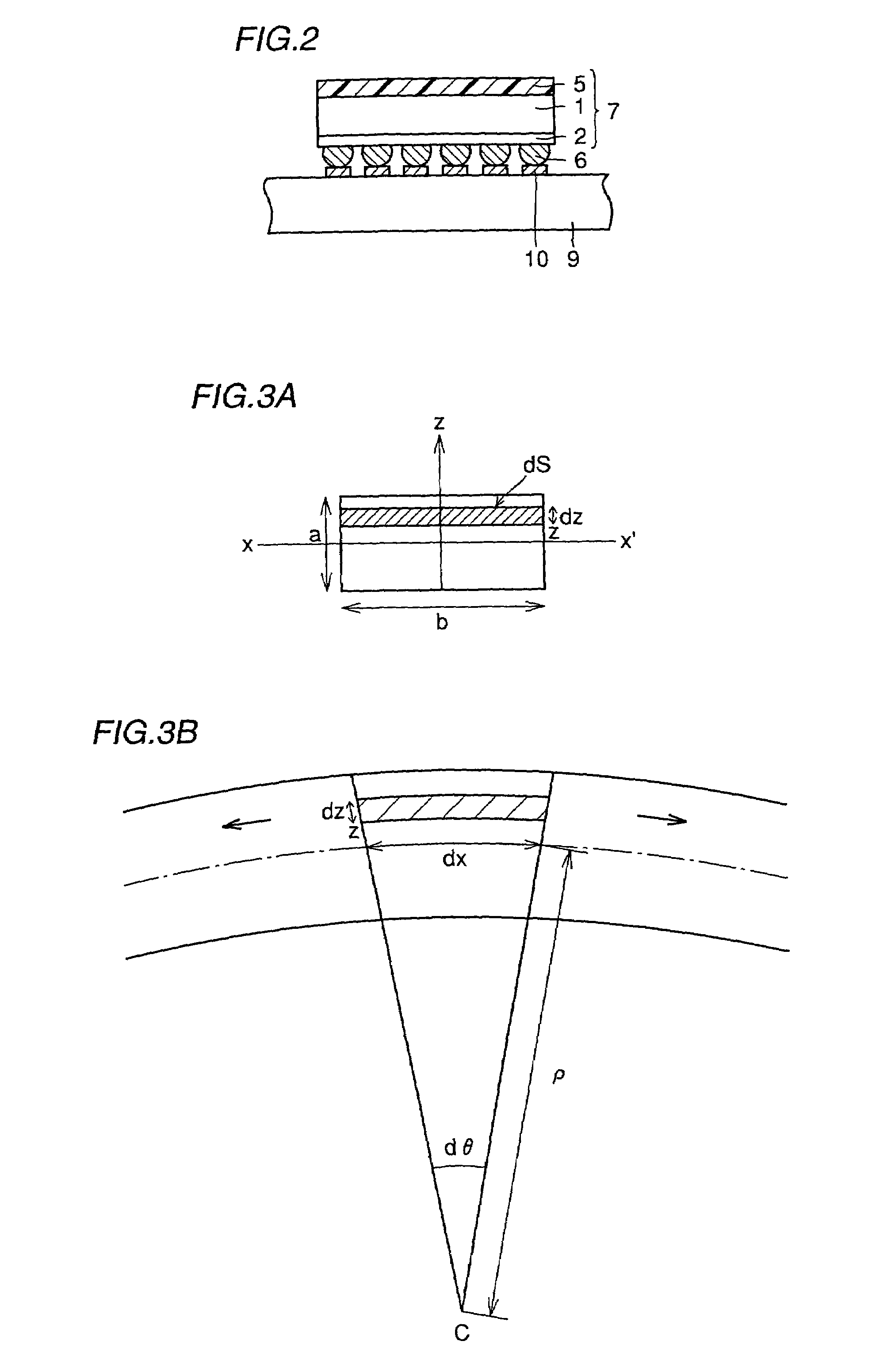
[0027]FIG. 3A shows a model in the form of a rectangular parallelepiped having a thickness a and a width b, as seen in cross section, applied to consider how LSI chip 7 bends. When this model is bent as shown in FIG. 3B, its upper side as seen in the figure expands due to tensility, its lower side as seen in the figure contracts due to pressure, and intermediate therebetween exists a neutral layer which neither expands nor contracts. Assuming that on average the model's expansion and contraction are balanced, the neutral layer includes the barycenter of the cross section. If the neutral layer has a small portion dx forming an angle dθ with respect to a center of curvature C and having a radius of curvature ρ then a thin layer dz spaced from the neutral layer by a distance z and having an area dS, which is equal to bdz, in cross section has an expansion rate of:

[(ρ+z)dθ−ρdθ] / ρdθ=z / ρ  (1).

As such, this layer experiences a tensility dT of E(z / ρ)dS. If a stick neither expands nor contra...

second embodiment

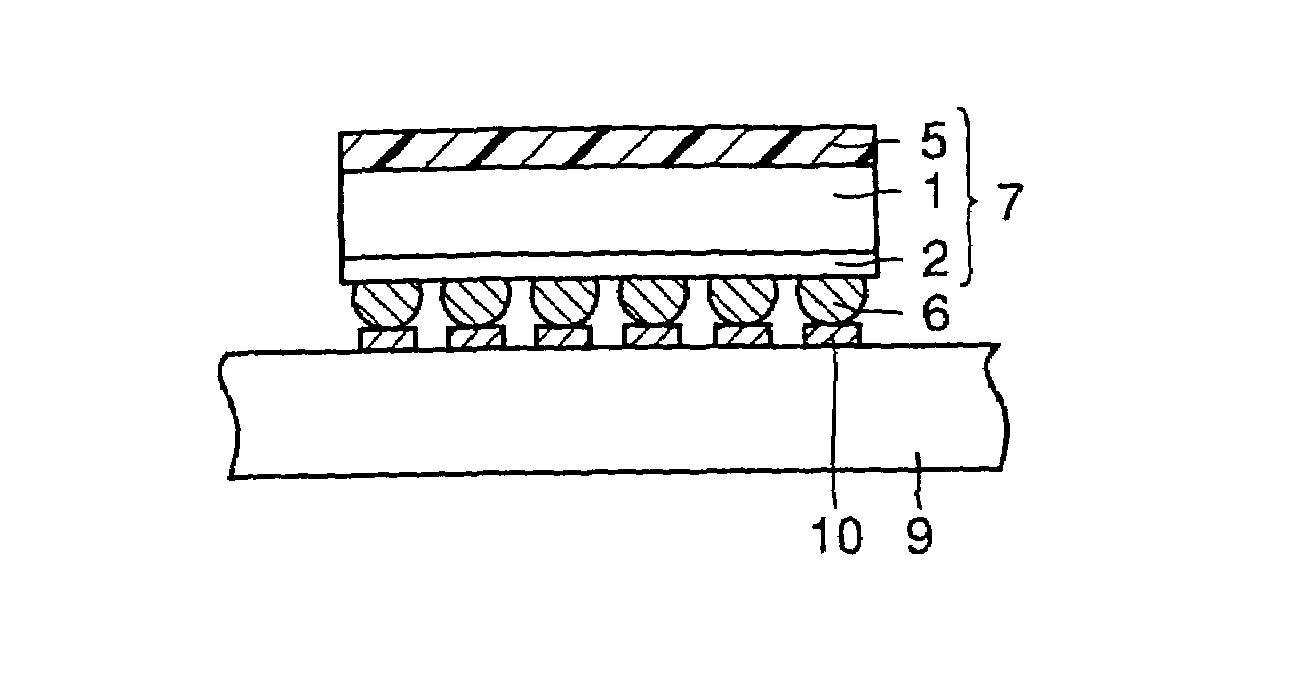
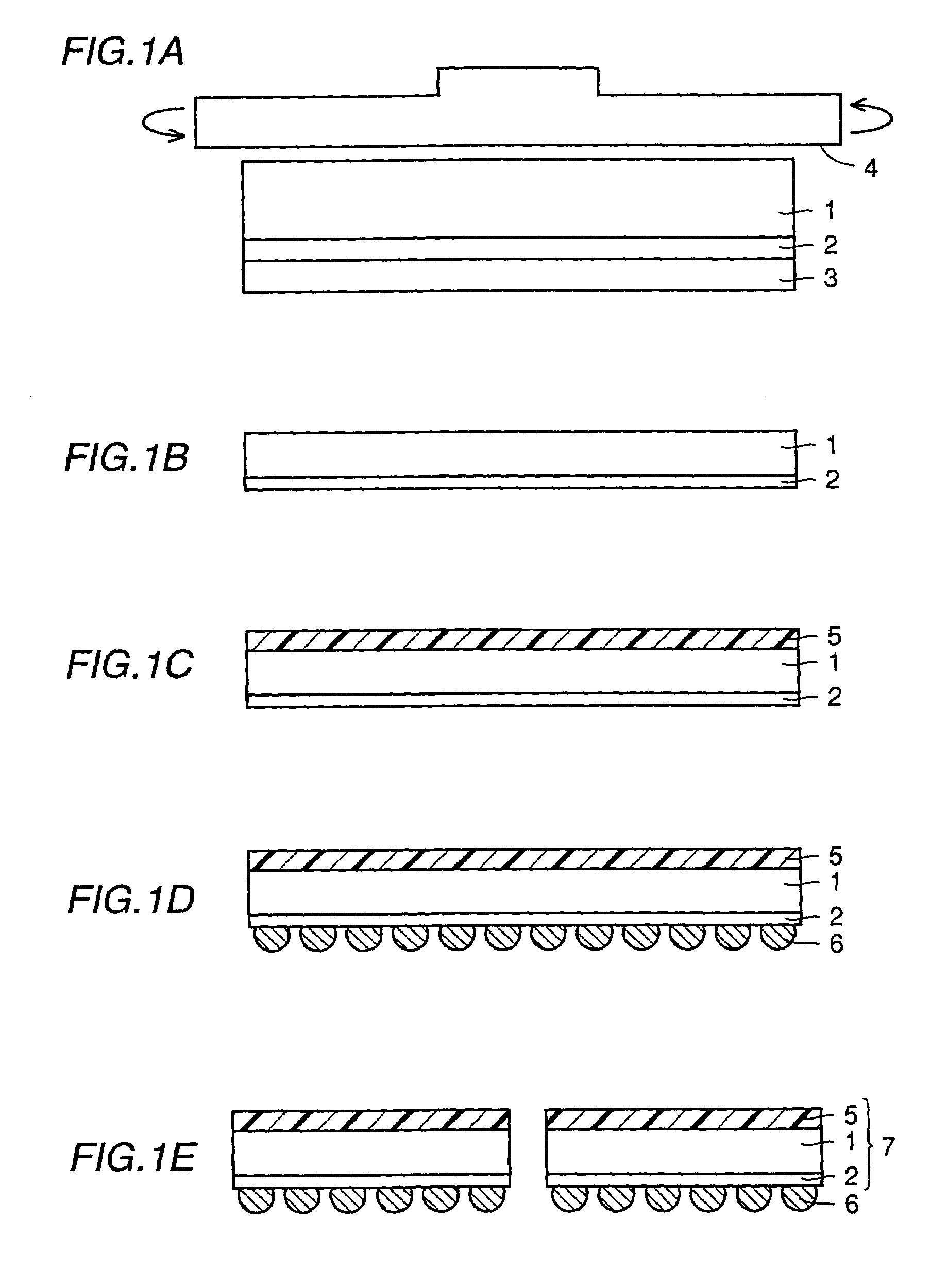
[0056]The present embodiment shows by way of example the FIG. 1E semiconductor chip 7 bare-chip packaged on printed circuit board 9. As a result, such a structure as shown in FIG. 2 is obtained.

[0057]The present embodiment can provide a semiconductor device wherein semiconductor chip 7 has a surface provided with an external connection electrode and a surface opposite that with the external connection electrode, abrased to reduce semiconductor chip 7 in thickness to allow the chip itself to flex in response to bending-force. As such, when printed circuit board 9 with semiconductor chip 7 packaged thereon receives force and thus bends, together with printed circuit board 9 semiconductor chip 7 can accordingly bend to alleviate stress in solder ball 6 or a solder connection so as to prevent the solder connection from breaking.

[0058]Furthermore, applying resin of a low elastic modulus (a low Young's modulus) on the abrased surface of semiconductor chip 7, can reinforce thus-configured ...


PUM


Abstract

A semiconductor package providing with a printed circuit board and a semiconductor device, including a semiconductor substrate having a surface provided with an external connection electrode and mounted on the printed circuit board, and, a surface opposite that with said external connection electrode, abrased with a mirror finish and reinforced with a back-surface reinforcement.

Description

CROSS REFERENCE[0001]This application is a Continuation of application Ser. No. 09 / 782,180, filed on Feb. 14, 2001 now abandoned. The present application claims priority to Japanese Patent Application No. 2000-034855, filed Feb. 14, 2000, the entire contents of which are hereby incorporated by reference.BACKGROUND OF THE INVENTION[0002]1. Field of the Invention[0003]The present invention relates generally to semiconductor devices and particularly to semiconductor devices that can be packaged with enhanced anti-bendability.[0004]2. Description of the Background Art[0005]In recent years, semiconductor devices have been further reduced in size and further increased in density to meet a demand for smaller and lighter mobile phones, mobile information equipment and other similar electronics and electronic equipment. To meet this demand there has been proposed bare-chip packaging, a technique applied in mounting an LSI chip directly on a printed circuit board.[0006]Reference will now be m...

Claims


Application Information

Patent Timeline
Patent Type & Authority Patents(United States)
IPC IPC(8): H01L23/48H01L23/52H01L29/40H01L21/02H01L21/60H01L21/304H01L23/28H01L23/29H01L23/31
CPCH01L23/293H01L23/296H01L23/3171H01L2224/16H01L2924/01322H01L2924/01004H01L2924/01012H01L2924/01078H01L2924/3511H01L2224/274
Inventor SUMIKAWA, MASATOTANAKA, KAZUMI
Owner SHARP KK
Why Eureka
Try Eureka