
Phase/frequency detector and charge pump architecture for referenceless clock and data recovery (CDR) applications

Inactive Publication Date: 2010-04-06
INTEL CORP
View PDF1 Cites 13 Cited by
  • Summary
  • Abstract
  • Description
  • Claims
  • Application Information

AI Technical Summary

Benefits of technology

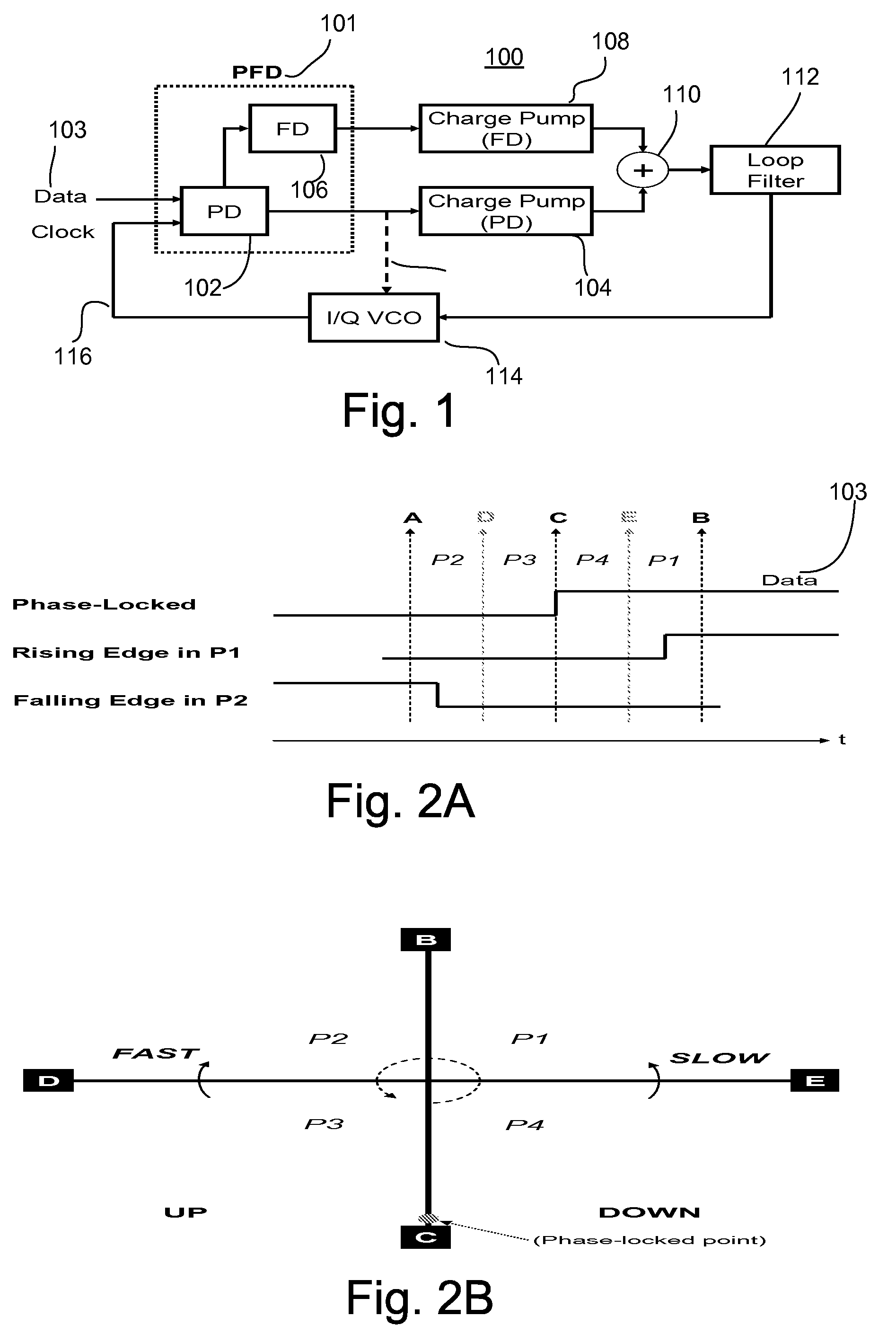
The present invention relates to clock and data recovery (CDR) circuits, which are important for high-speed data transmission and processing. CDR circuits require operating at high speeds, such as tens of gigabits per second. The invention proposes a new CDR circuit design that can recover both timing and phase information from the data stream using a combination of a phase / frequency detector and a conditionally closed loop. The CDR circuit can operate at high speeds and can be used in retimer applications where there is no external reference clock. The invention also includes several different types of PD structures and methods for controlling the VCO to improve the performance of the CDR circuit.

Problems solved by technology

However, when such a reference clock source is not easily available, e.g. in retimer applications, referenceless CDR circuits may be necessary, which can perform both frequency acquisition and phase locking solely based on the incoming data stream.

Method used


Image

  • Phase/frequency detector and charge pump architecture for referenceless clock and data recovery (CDR) applications
  • Phase/frequency detector and charge pump architecture for referenceless clock and data recovery (CDR) applications
  • Phase/frequency detector and charge pump architecture for referenceless clock and data recovery (CDR) applications

Examples


first embodiment

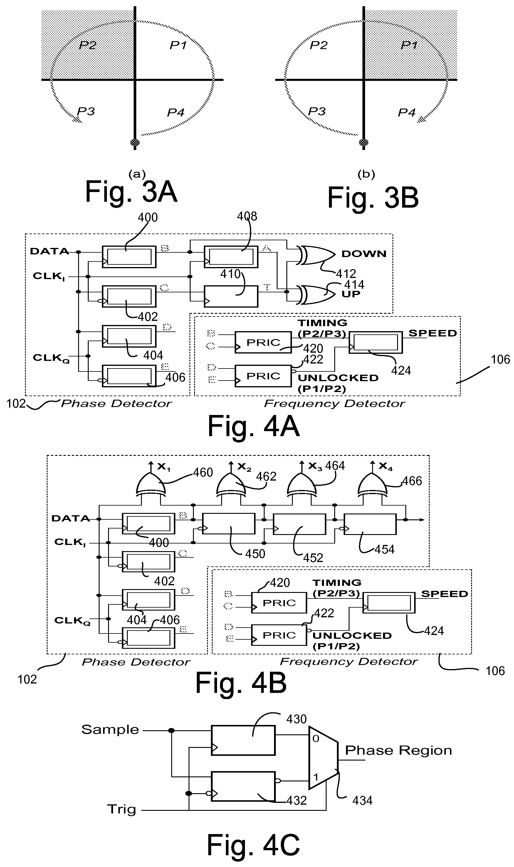
[0037]Referring now to FIG. 5B, the tri-state FD charge pump 104 comprises a differential pair 520, 522 and current mirrors 531, 537 and 532, 538 to deliver a tail current of 2×ICP-FD. When SPEED is high, transistor 537 is driven to sink a current of 2×ICP-FD, while transistor 538 sinks zero current. The cascaded differential pairs 524, 526 and 533, 534 perform logic AND operation to select the phase region P1 such that the charge pump drains a current of 2×ICP-FD from the X node only when the phasor falls within P1. On the other hand, when SPEED is low, transistor 537 is driven to sink zero current, while transistor 538 sinks a current of 2×ICP-FD. The cascaded differential pairs 528, 530 and 535, 536 perform logic AND operation to select the phase region P2 such that the charge pump drains a current of 2×ICP-FD from the Y node only when the phasor falls within P2.

second embodiment

[0038]Referring now to FIG. 5C, the tri-state FD charge pump 104 comprises a differential pair 552, 554 to draw a current of 2×ICP-FD to starve tail current sources 572 or 574. When SPEED is high, it draws a current of 2×ICP-FD to starve tail current source 574, while drawing none from tail current source 572. The differential pairs 556, 558 and 560, 562 performs logic AND operation to select the phase region P1 such that the charge pump drains a current of 2×ICP-FD from the X node only when the phasor falls within P1. On the contrary, when SPEED is low, tail current source 572 is starved. The cascaded differential pairs 564, 566 and 568, 570 perform logic AND operation to select the phase region P2 such that the charge pump drains a current of 2×ICP-FD from the Y node only when the phasor falls within P2.

[0039]Either FD charge pump from FIGS. 5B or 5C may be adopted in the CDR loop. The FD charge pumps 108 are conditionally active only within either P1 or P2, shown as gray areas in...


PUM


Abstract

A stream of data may flow over a fiber or other medium without any accompanying clock signal. The receiving device may then be required to process this data synchronously. Embodiments describe clock and data recovery (CDR) circuits which may sample a data signal at a plurality of sampling points to partition a clock cycle into four phase regions P1, P2, P3, and P4 which may be represented on a phase plane being divided into four quadrants. A relative phase between a data signal transition edge and a clock phase may be represented by a phasor on the phase plane. The clock phase and frequency may be adjusted by determining the instantaneous location of the phasor and the direction of phasor rotation in the phase plane.

Description

FIELD OF THE INVENTION[0001]Embodiments of the present invention may relate to logic circuits and, more particularly, embodiments of the present invention may relate to clock and data recovery circuits.BACKGROUND INFORMATION[0002]In many electronic systems, data may be transmitted or retrieved without any timing reference. For example, in optical communications, a stream of data may flow over a fiber without any accompanying clock signal. The receiving device may then be required to process this data synchronously. Therefore, the clock or timing information must be recovered from the data at the receiver using clock and data recovery (CDR) circuits. With the rapid growth of electrical and optical link capability, CDR circuits may require operating at high speeds such as tens of gigabits per second (Gbits / second).[0003]Further, clock and data recovery (CDR) circuits are important for modern transceiver systems to reduce jitter and improve signal quality. Phase-locked-loop (PLL)-based...

Claims


Application Information

Patent Timeline
Patent Type & Authority Patents(United States)
IPC IPC(8): G01R23/06H03D13/00
CPCH03L7/087H03L7/0896H04L7/033H03L7/113H03L7/091H03L7/00
Inventor HSUEH, YU-LIGAO, MIAOBINLIU, CHIEN-CHANG
Owner INTEL CORP
Learn More