

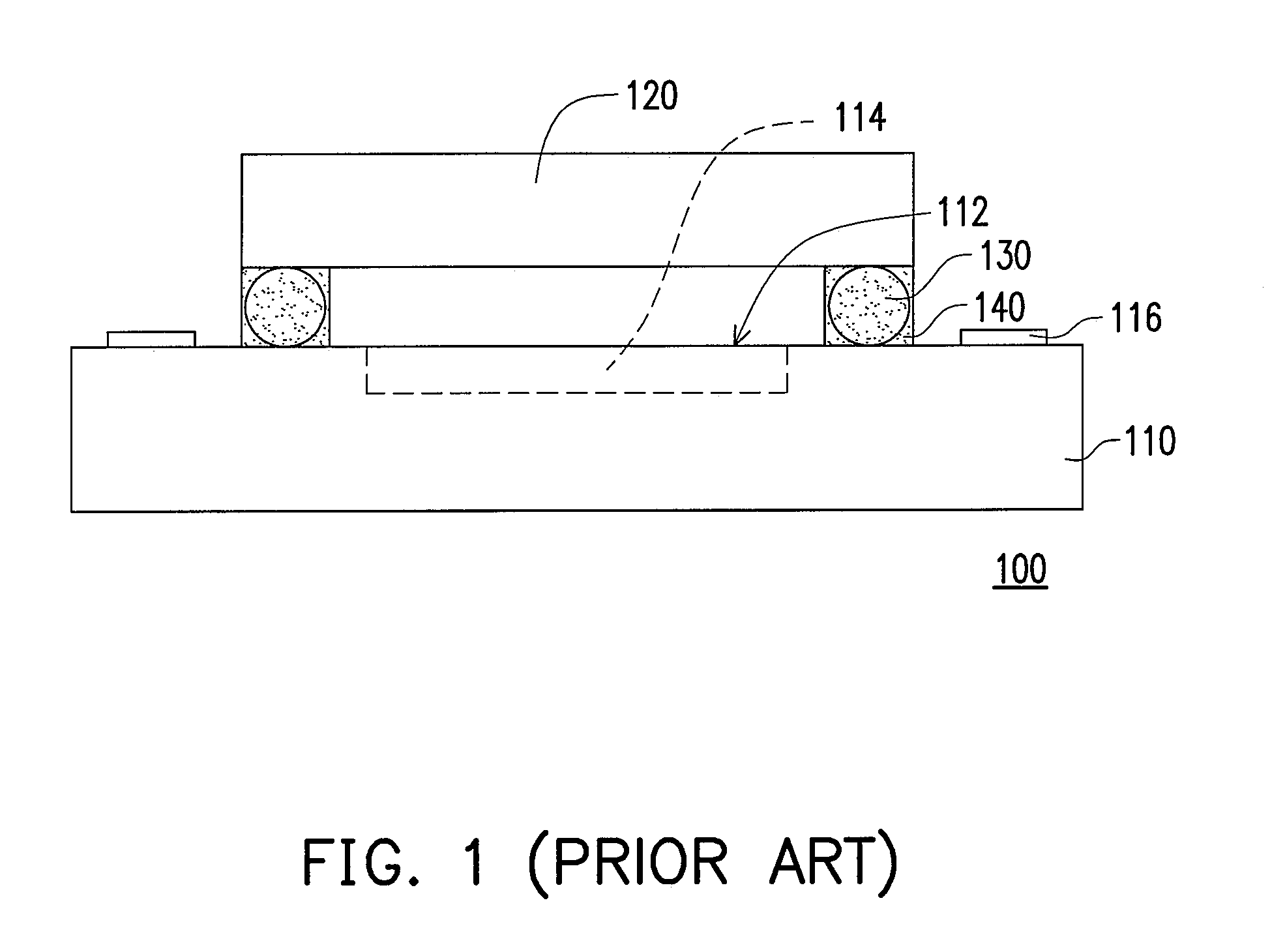
Wafer-level chip packaging process and chip package structure
a packaging process and chip technology, applied in the direction of electrical equipment, semiconductor devices, semiconductor/solid-state device details, etc., can solve the problems of low process yield and high cost of foregoing packaging process, so as to reduce the possibility of particles scratching or contaminating an active surface, and reduce the possibility of voids or bubbles
- Summary
- Abstract
- Description
- Claims
- Application Information
AI Technical Summary
Benefits of technology
Problems solved by technology
Method used
Image

Examples
Embodiment Construction
[0027]Reference will now be made in detail to the present preferred embodiments of the invention, examples of which are illustrated in the accompanying drawings. Wherever possible, the same reference numbers are used in the drawings and the description to refer to the same or like parts.
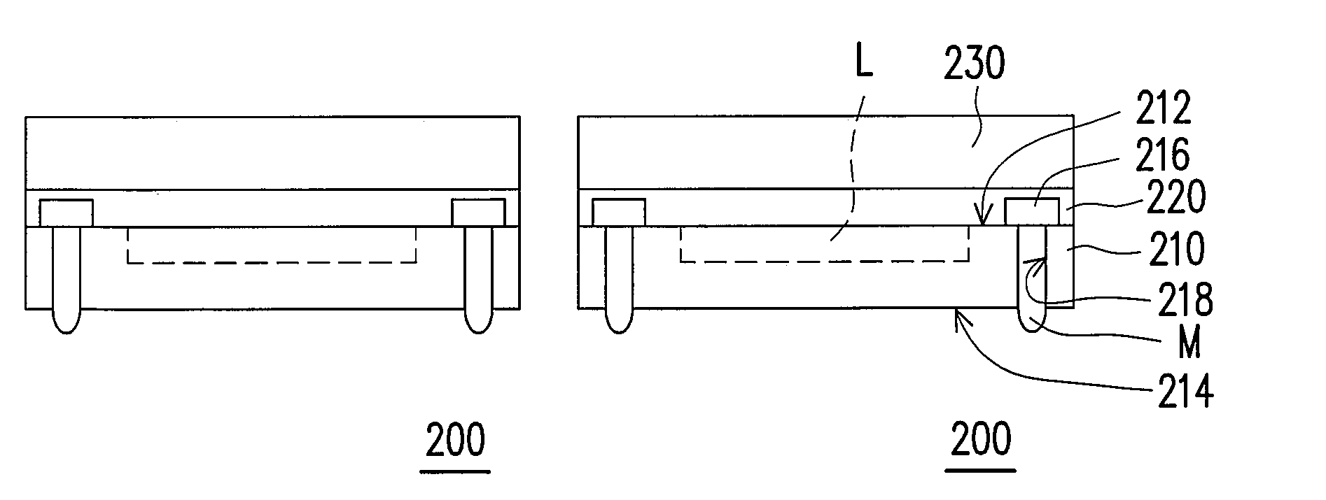
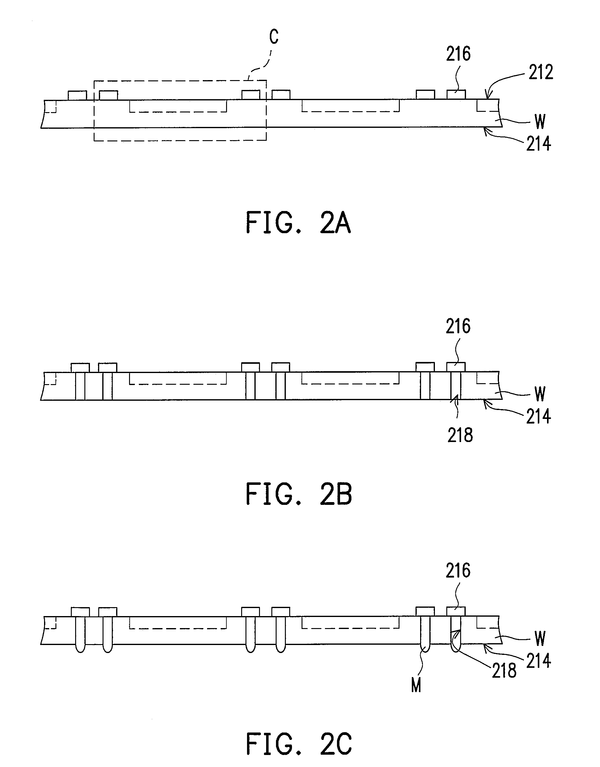
[0028]FIGS. 2A through 2F are side and schematic views showing the steps in a wafer-level chip packaging process. The wafer-level chip packaging process in the present embodiment includes the following steps. First, as shown in FIG. 2A, a wafer W is provided. The wafer W includes a plurality of chip units C. Furthermore, the wafer W has an active surface 212 and an opposite back surface 214. A plurality of pads 216 are disposed on the active surface 212. The material forming the pads 216 includes aluminum, for example.
[0029]Next, as shown in FIG. 2B, a plurality of through holes 218 are formed under the pads 216. In the present embodiment, the method of forming the through holes 218 includes etching,...
PUM
 Abstract
Description
Claims
Application Information