
Analog-to-digital converter having reduced number of activated comparators

a technology of analog-to-digital converter and comparator, applied in the field of electrical and electronic arts, can solve the problems of increasing the resolution, increasing the likelihood that the adc output will not be a pure thermometer code, and increasing the complexity of the encoder in the adc system, so as to achieve the effect of reducing the power consumption of the adc circui

Active Publication Date: 2010-04-13
AVAGO TECH INT SALES PTE LTD
View PDF7 Cites 32 Cited by
  • Summary
  • Abstract
  • Description
  • Claims
  • Application Information

AI Technical Summary

Benefits of technology

[0008]Illustrative embodiments of the present invention meet the above-noted need by providing circuits, methods and techniques for advantageously reducing power consumption in an ADC circuit without significantly degrading performance of the ADC circuit, such as, for example, resolution. To accomplish this, embodiments of the invention beneficially reduce the number of comparators that are activated (e.g., turned on) during any given sample period and dynamically control corresponding reference signal levels supplied to the comparators.
[0010]In accordance with another aspect of the invention, a method for reducing power consumption in an ADC circuit is provided. The method includes the steps of: defining a plurality of regions into which an analog input signal applied to the ADC circuit is quantized; performing at least one of: activating a subset of the plurality of comparators during a given sample period; and controlling levels of the corresponding reference signals of the comparators as a function of a level of the input signal; and generating an output signal as a function of respective outputs of active comparators in the ADC circuit during a given sample period, the output signal for the given sample period being a digital representation of the analog input signal. A number of active comparators during the given sample period is no greater than one less than a number of regions into which the input signal is quantized.

Problems solved by technology

However, increased resolution also increases the likelihood that the ADC output will not be a pure thermometer code.
This may result from, for example, noise and offsets due to process, voltage, temperature, etc. being larger than the difference in adjacent reference levels between two comparators in the ADC, thus causing a comparator to make an incorrect decision.
Consequently, the complexity of an encoder in an ADC system becomes prohibitive in terms of both the hardware required to encode the output of the ADC and the latency of the encoding computation.
Furthermore, for each additional encoded bit of the digitized code, twice the number of comparators is needed, thereby increasing the power and / or area of the ADC, which is undesirable.
Unfortunately, if an incorrect decision is made during some bit period, the error will likely accumulate to cause more incorrect decisions.
ML detectors are disadvantageous primarily because they require substantial hardware to implement.
Unfortunately, signal shaping techniques often add significant noise to the signal, which is undesirable.
Even aggressive pre-emphasis may not be sufficient in many systems to permit the receiver to recover the proper bit sequence.

Method used


Image

  • Analog-to-digital converter having reduced number of activated comparators
  • Analog-to-digital converter having reduced number of activated comparators
  • Analog-to-digital converter having reduced number of activated comparators

Examples


Embodiment Construction

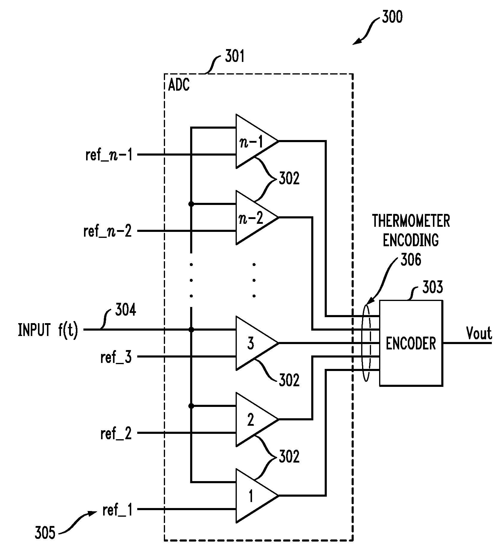
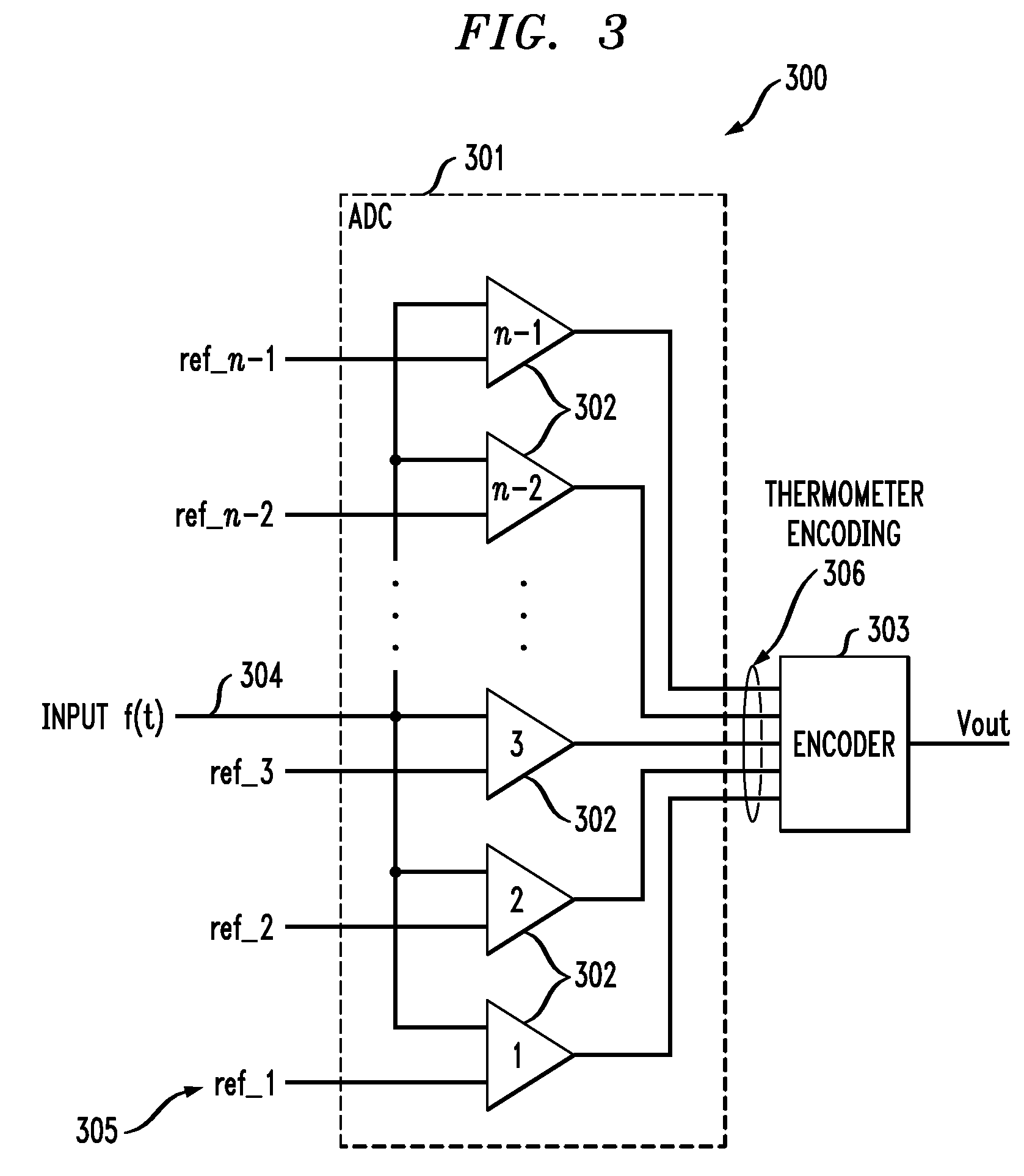
[0024]The present invention will be described herein in the context of exemplary ADC circuits, systems and method for use therewith. It is to be understood, however, that the techniques of the present invention are not limited to the circuits, systems and method shown and described herein. Rather, embodiments of the invention are directed to techniques for reducing power consumption in an ADC circuit without significantly impacting performance (e.g., resolution) and / or area of the circuit. Although preferred embodiments of the invention may be fabricated in a silicon wafer, embodiments of the invention can alternatively be fabricated in wafers comprising other materials, including but not limited to gallium arsenide (GaAs), indium phosphide (InP), etc.

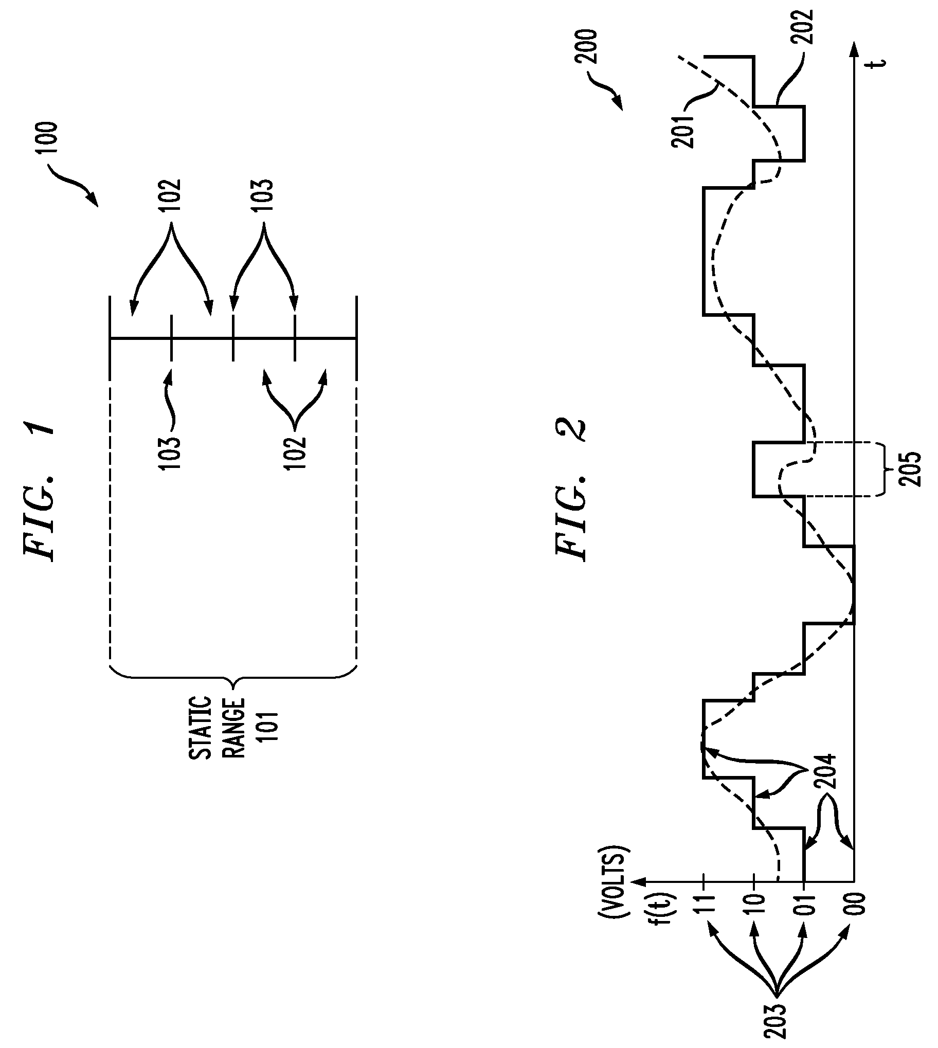
[0025]FIG. 1 is an exemplary diagram 100 illustrating one method of dividing a static signal range into multiple regions. With reference to FIG. 1, an ADC operates over a static (fixed), specified input signal range 101. Usually the st...


PUM


Abstract

An ADC circuit includes multiple comparators and a controller coupled to the comparators. Each of the comparators is operative to generate an output indicative of a difference between a first signal representative of an input signal applied to the ADC circuit and a corresponding reference signal. The controller is operative to perform at least one of: (i) activating a subset of the comparators during a given sample period being; and (ii) controlling levels of the corresponding reference signals of the comparators as a function of a level of the input signal. A number of active comparators during the given sample period is no greater than one less than a number of regions into which the input signal is quantized.

Description

FIELD OF THE INVENTION[0001]The present invention relates generally to the electrical and electronic arts, and more particularly relates to analog-to-digital conversion.BACKGROUND OF THE INVENTION[0002]An analog-to-digital converter (ADC) is a circuit that samples and converts an analog signal to a digital signal. With respect to the allowable or meaningful signal values, an analog signal is continuous while a digital signal is discrete or quantized. Usually, the signals are represented by voltage levels, varying in a continuous fashion over some specified voltage range for analog signals and discrete specified quantized levels for digital signals. An important characteristic of an ADC is its resolution, which is a function of the number of quantized voltage levels to which the analog input signal may be assigned. Resolution thus describes the fineness of the quantization performed by the ADC. Generally, the higher the resolution of the ADC, the more accurate the digital representat...

Claims


Application Information

Patent Timeline
Patent Type & Authority Patents(United States)
IPC IPC(8): H03M1/36
CPCH03M1/182H03M1/002H03M1/004H03M1/367H03M1/361
Inventor CHMELAR, ERIKITO, CHOSHU
Owner AVAGO TECH INT SALES PTE LTD
Learn More