Method and system for model-based design and layout of an integrated circuit

a technology of integrated circuits and models, applied in computer aided design, program control, instruments, etc., can solve the problems of reducing the execution time of pv tools, the inability to work for the intended purpose of silicon products, and the complexity and number of transistors, so as to limit the amount of resources consumed by drc processing and achieve high degree of manufacturability

Active Publication Date: 2010-04-13
CADENCE DESIGN SYST INC
View PDF38 Cites 6 Cited by
  • Summary
  • Abstract
  • Description
  • Claims
  • Application Information

AI Technical Summary

Benefits of technology

[0008]DRC tools typically read and manipulate a design database which stores information about device geometries and connectivity. Because compliance with design rules generally constitutes the gating factor between one stage of the design and the next, DRC tools are typically executed multiple times during the evolution of the design and contribute significantly to the project's critical path. Therefore, reducing DRC tool execution time makes a major contribution to the reduction of overall design cycle times.
[0009]As the quantity of data in modern IC designs become larger and larger over time, the execution time required to process DRC tools upon these IC designs also becomes greater. The goal of reducing PV tool execution time is in sharp tension with many modern IC designs being produced by electronics companies that are constantly increasing in complexity and number of transistors. The more transistors and other structures on an IC design, the greater amounts of time that is normally needed to perform DRC processing. This problem is exacerbated by constantly improving IC manufacturing technologies that can create IC chips at ever-smaller feature sizes, which allows increasingly greater quantities of transistors to be placed within the same chip area, as well resulting in more complex physical and lithographic effects during manufacture.
[0012]The present invention is a method, system, and computer program product for model-based method for placement and routing. Models are used to guide the placement and routing of polygons on the IC layout. In effect, the parameters that are used for placement and routing are guided by the model data so that the layout can be formed with a high degree of manufacturability from the outset.

Problems solved by technology

Violating a single foundry rule can result in a silicon product that does not work for its intended purpose.
The goal of reducing PV tool execution time is in sharp tension with many modern IC designs being produced by electronics companies that are constantly increasing in complexity and number of transistors.
The more transistors and other structures on an IC design, the greater amounts of time that is normally needed to perform DRC processing.
This problem is exacerbated by constantly improving IC manufacturing technologies that can create IC chips at ever-smaller feature sizes, which allows increasingly greater quantities of transistors to be placed within the same chip area, as well resulting in more complex physical and lithographic effects during manufacture.
In addition, DRC rules often contain design constraints that are much more limiting than are needed for any particular design or portion of a design.
However, certain IC design may actually need parameters that are more or less cautious than other designs.
Since DRC rules typically operate on an “all or nothing” basis, this means that many IC design may fail DRC processing even though they would function properly for intended purposes if manufactured.

Method used


Image

  • Method and system for model-based design and layout of an integrated circuit
  • Method and system for model-based design and layout of an integrated circuit
  • Method and system for model-based design and layout of an integrated circuit

Examples


Embodiment Construction

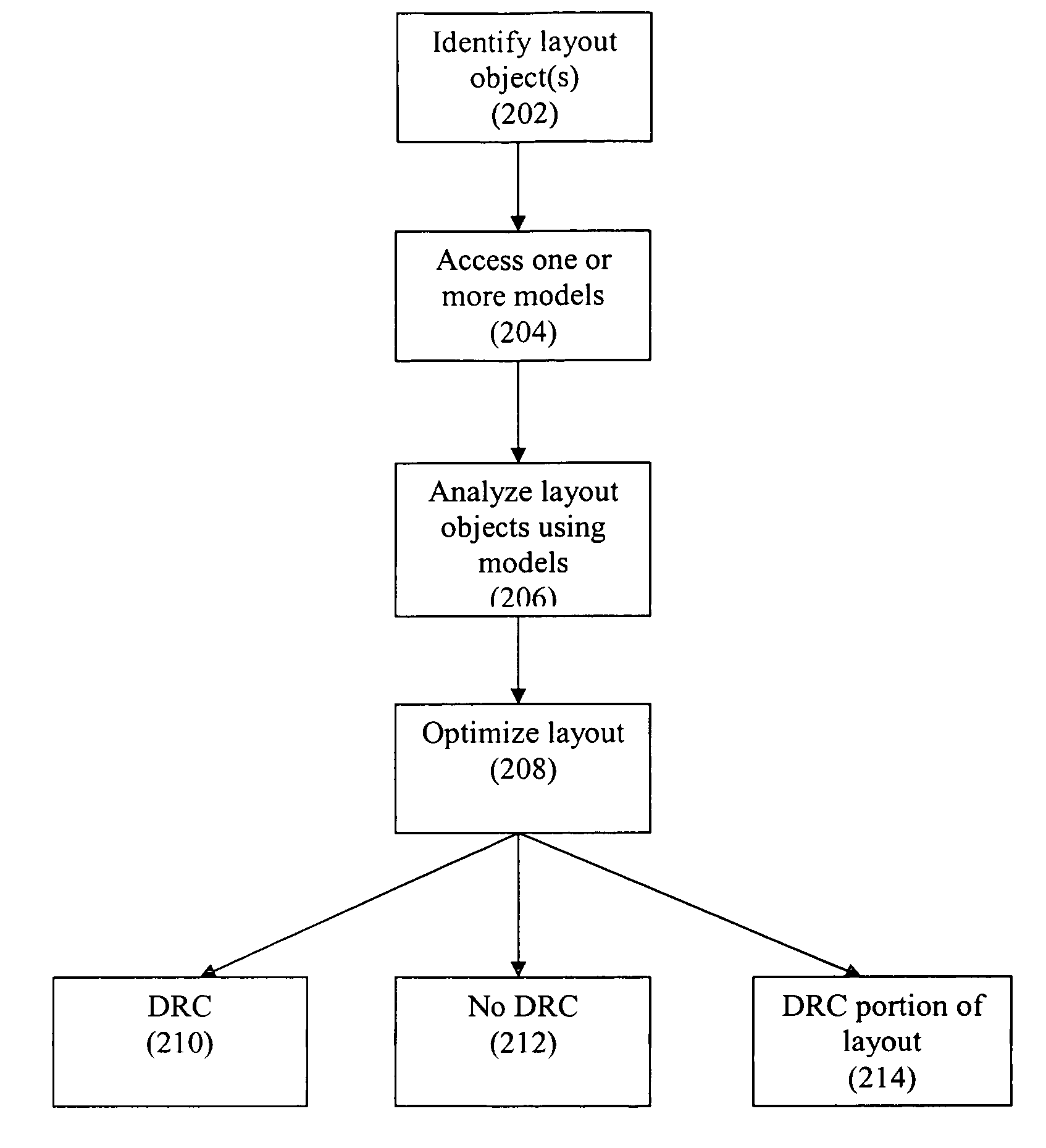
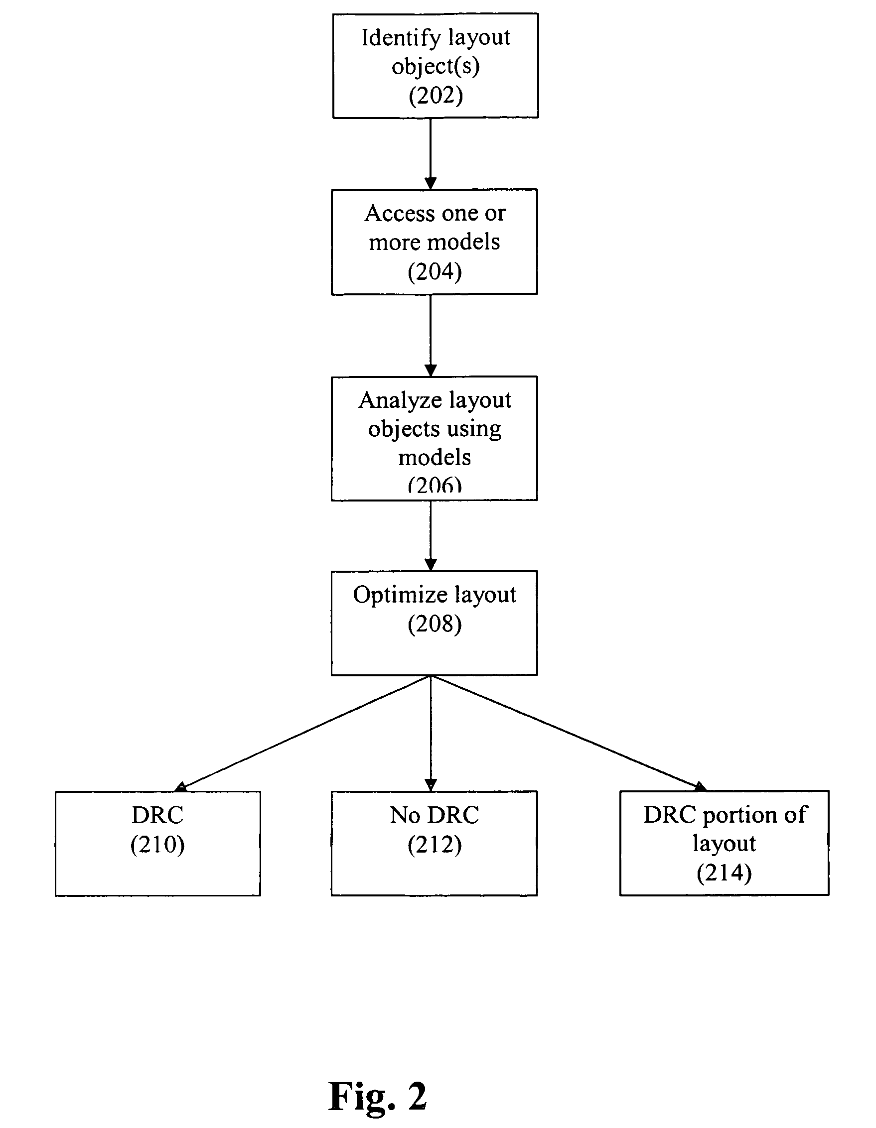
[0018]The present approach is directed to a model-based method for placement and routing. As used herein, the term “Model” refers to a set of data that identifies one or more specific characteristics within an IC layout and data relating to its effect, manufacturability, and / or usability. For example, a model may present a defined characteristic such as “spacing” and a chart or numeric data indicating the probability of failure / success at different spacing values.

[0019]With the present invention, models are used to guide the placement and routing of polygons on the IC layout. In effect, the parameters that are used for placement and routing are guided by the model data so that the layout can be formed with a high degree of manufacturability from the outset. The parameter values can be selected based upon the specific type of design that is being operated upon, so that the layout is optimized for the specific circuit being designed. This can significantly improve upon the “one size f...


PUM


Abstract

Disclosed is a method, system, and computer program product for implementing model-based layout, placement, and routing. Models are used to guide the placement and routing of polygons on the IC layout. In effect, the parameters that are used for placement and routing are guided by the model data so that the layout can be formed with a high degree of manufacturability from the outset.

Description

BACKGROUND AND SUMMARY[0001]The invention is directed to a more efficient approach for implementing layout, placement, and routing of integrated circuit designs.[0002]A semiconductor integrated circuit (IC) has a large number of electronic components, such as transistors, logic gates, diodes, wires, etc., that are fabricated by forming layers of different materials and of different geometric shapes on various regions of a silicon wafer.[0003]The various components of an integrated circuit are initially defined by their functional operations and relevant inputs and outputs. From the HDL or other high level description, the actual logic cell implementation is typically determined by logic synthesis, which converts the functional description of the circuit into a specific circuit implementation. The logic cells are then “placed” (i.e., given specific coordinate locations in the circuit layout) and “routed” (i.e., wired or connected together according to the designer's circuit definitio...

Claims


Application Information

Patent Timeline
Patent Type & Authority Patents(United States)
IPC IPC(8): G06F17/50
CPCG06F17/5077G06F17/5072G06F30/392G06F30/394G06F2119/18
Inventor NEQUIST, ERICBRASHEARS, RICHARD
Owner CADENCE DESIGN SYST INC
Why Eureka
Try Eureka