SOI-based tunable laser

a technology of tunable lasers and silicon-based insulators, which is applied in the direction of semiconductor lasers, laser details, electrical equipment, etc., can solve the problems of high inventory requirements, high cost of those systems, and disturbing the ability to “tune” the laser over the desired wavelength range, so as to achieve improved thermal isolation

Active Publication Date: 2010-04-20
CISCO TECH INC
View PDF4 Cites 40 Cited by
  • Summary
  • Abstract
  • Description
  • Claims
  • Application Information

AI Technical Summary

Benefits of technology

[0010]In accordance with the present invention, a gain medium (such as, for example, a semiconductor optical amplifier) is disposed within a cavity etched within a SOI substrate. A tunable wavelength reflecting element and associated phase matching element are formed on the surface of the SOI structure, with optical waveguides formed in the surface SOI layer providing the communication between these components. The tunable wavelength element is controlled to adjust the optical wavelength. Separate discrete lensing elements may be disposed in the cavity with the gain medium, providing efficient coupling of the optical signal into the SOI waveguides. Alternatively, the gain medium itself may be formed to include spot converting tapers on its endfaces, the tapers used to provide mode matching into the associated optical waveguides.
[0012]It is an aspect of the present invention that the positioning of the gain medium within a recessed cavity provides improved thermal isolation between the gain medium and the remainder of the optical components of the laser.

Problems solved by technology

The high inventory requirement contributes to the high cost of those systems.
One difficulty with many of the conventional prior art tunable lasers, however, is that they require a number of discrete components, these components each having a number of surfaces that may introduce stray, unwanted reflections into the laser, disturbing the ability to “tune” the laser over the desired wavelength range.

Method used


Image

  • SOI-based tunable laser
  • SOI-based tunable laser
  • SOI-based tunable laser

Examples


Embodiment Construction

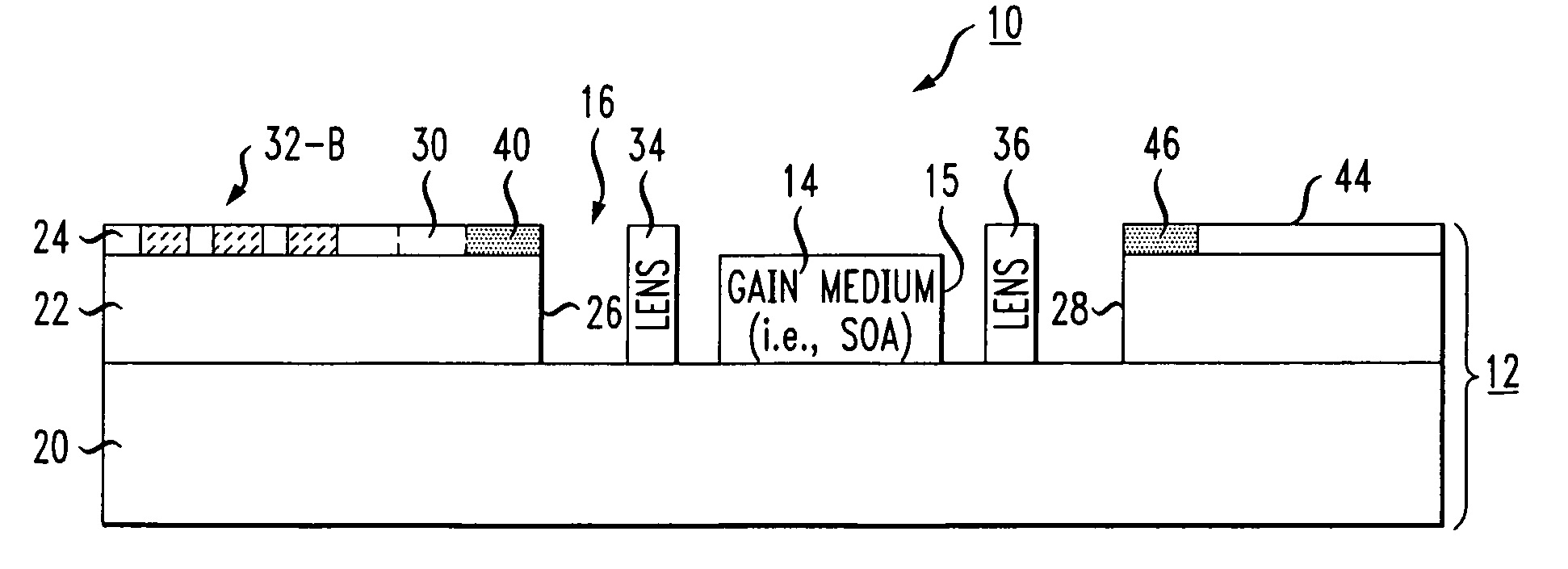
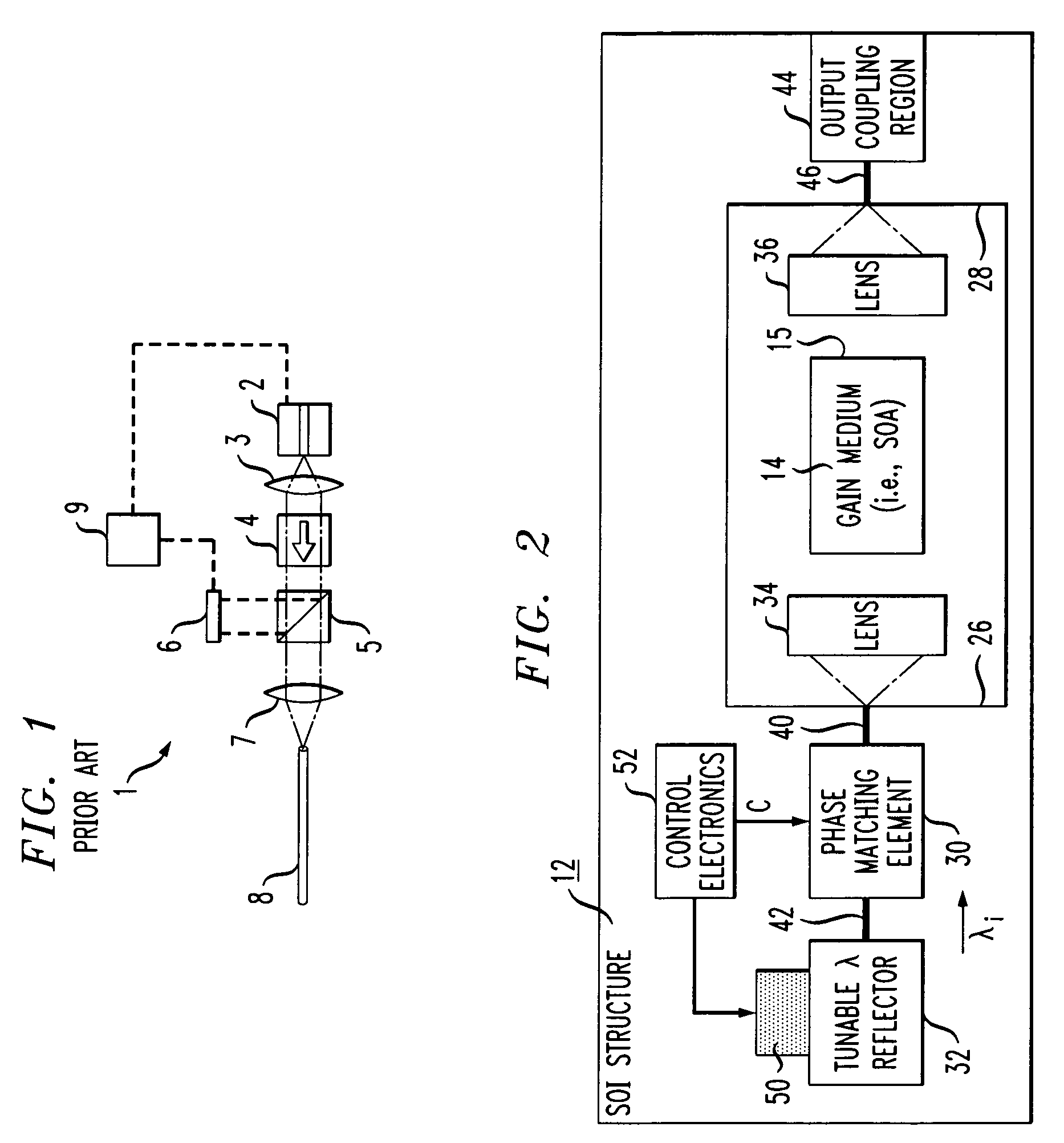
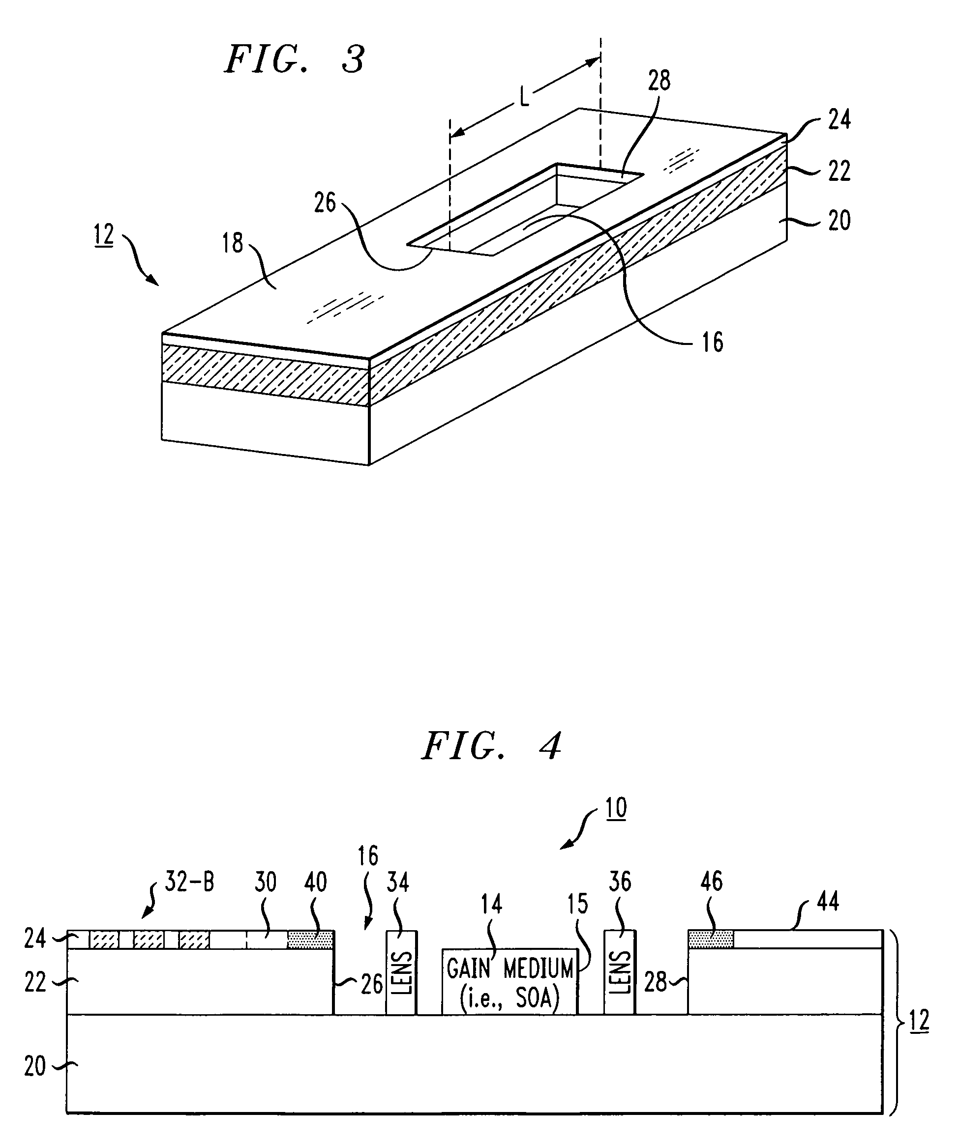
[0021]FIG. 2 is a top view of an exemplary SOI-based tunable laser 10 formed in accordance with the present invention within an SOI structure 12. Tunable laser 10 includes a gain medium 14, such as a semiconductor optical amplifier, disposed within a cavity 16 formed through a top surface 18 of SOI structure 12. FIG. 3 is an isometric view of exemplary SOI structure 12 within which an exemplary laser cavity 16 is formed. As best shown in FIG. 3, SOI structure 12 comprises a silicon substrate 20, a dielectric layer 22 formed over substrate 20 and a relatively thin silicon surface layer 24 (hereinafter referred to as “SOI layer 24”) disposed over dielectric layer 22. As with many other SOI-based optical arrangements currently being developed, SOI layer 24 is used as the waveguiding layer to support the transmission of optical signals within tunable laser 10 in the manner to be described in detail below.

[0022]Advantageously, the use of silicon materials in the formation of structure 12...


PUM


Abstract

A silicon-on-insulator (SOI)-based tunable laser is formed to include the gain medium (such as a semiconductor optical amplifier) disposed within a cavity formed within the SOI substrate. A tunable wavelength reflecting element and associated phase matching element are formed on the surface of the SOI structure, with optical waveguides formed in the surface SOI layer providing the communication between these components. The tunable wavelength element is controlled to adjust the optical wavelength. Separate discrete lensing elements may be disposed in the cavity with the gain medium, providing efficient coupling of the optical signal into the SOI waveguides. Alternatively, the gain medium itself may be formed to include spot converting tapers on its endfaces, the tapers used to provide mode matching into the associated optical waveguides.

Description

CROSS-REFERENCE TO RELATED APPLICATIONS[0001]This application claims the benefit of U.S. Provisional Application No. 61 / 002,509, filed Nov. 9, 2007.TECHNICAL FIELD[0002]The present invention relates to a tunable laser and, more particularly, to a silicon-on-insulator (SOI)-based tunable laser with a gain medium disposed within a cavity formed within the SOI substrate.BACKGROUND OF THE INVENTION[0003]There is an increasing demand for tunable lasers given the advent of wavelength-division multiplexing (WDM) which has become widespread in fiber optic communication systems. WDM transponders include a laser, modulator, a receiver and associated electronics. One WDM transponder operates a fixed laser in the near-infrared spectrum at around 1550 nm. A 176 wavelength system uses one laser per wavelength and, therefore, such a system typically must store a 176 additional WDM transponders as “spares” to deal with failures. The high inventory requirement contributes to the high cost of those s...

Claims


Application Information

Patent Timeline
Patent Type & Authority Patents(United States)
IPC IPC(8): H01S3/10H01S3/13
CPCH01S5/141H01S5/021H01S5/02248H01S5/06256H01S5/02268H01S5/02325H01S5/02375
Inventor WEBSTER, MARKPIEDE, DAVIDGOTHOSKAR, PRAKASH
Owner CISCO TECH INC
Why Eureka
Try Eureka