Semiconductor device for RF switching

a technology of rf switching and semiconductor devices, which is applied in semiconductor devices, electronic switching, pulse techniques, etc., can solve the problems of compound semiconductors being used mainly as multifunctional or high-performance semiconductor switches, albeit expensive, and their performance, so as to suppress the leakage of rf signals and suppress the effect of leakag

Inactive Publication Date: 2010-05-04
RENESAS ELECTRONICS CORP
View PDF11 Cites 49 Cited by
  • Summary
  • Abstract
  • Description
  • Claims
  • Application Information

AI Technical Summary

Benefits of technology

[0016]According to the present invention, when the gate is turned off, the control unit applies a reverse bias to a portion between the source and the well, and the drain and the well. Hence, an area of a depletion layer formed at the junction can be increased. This makes it possible to reduce a capacitance at the junction between the source and the well and the junction between the drain and the well and to suppress the leakage of signals through a capacitance at the junction when the gate is turned off.
[0018]According to the present invention, the shunt transistor is provided, whereby even if the switching transistor is turned off, the signals are not output. Further, when the switching transistor is turned on, the shunt transistor is turned off. At this time, a voltage is applied such that the source and the drain are biased reversely to the well, making it possible to suppress the leakage of the signals to the shunt transistor. That is, according to the present invention, it is possible to provide a semiconductor device capable of suppressing leakage of RF signals at the time of turning on / off a switch.

Problems solved by technology

Further, a compound semiconductor is mainly used as a multifunctional or high-performance semiconductor switch albeit expensive.
However, the switch of this type has a disadvantage in that its performance, especially, isolation characteristic with high frequencies is inferior to that of the compound semiconductor and is required to improve its performance.
However, the inventors of this application find the following problems.
Therefore, the RF signal is unintentionally transmitted through these capacitances.
That is, the nMOSFET 100a of Related Art 1 has a problem in that the input RF signals are not completely blocked and are partially transmitted through the switching nMOSFET 100a.

Method used


Image

  • Semiconductor device for RF switching
  • Semiconductor device for RF switching
  • Semiconductor device for RF switching

Examples


first embodiment

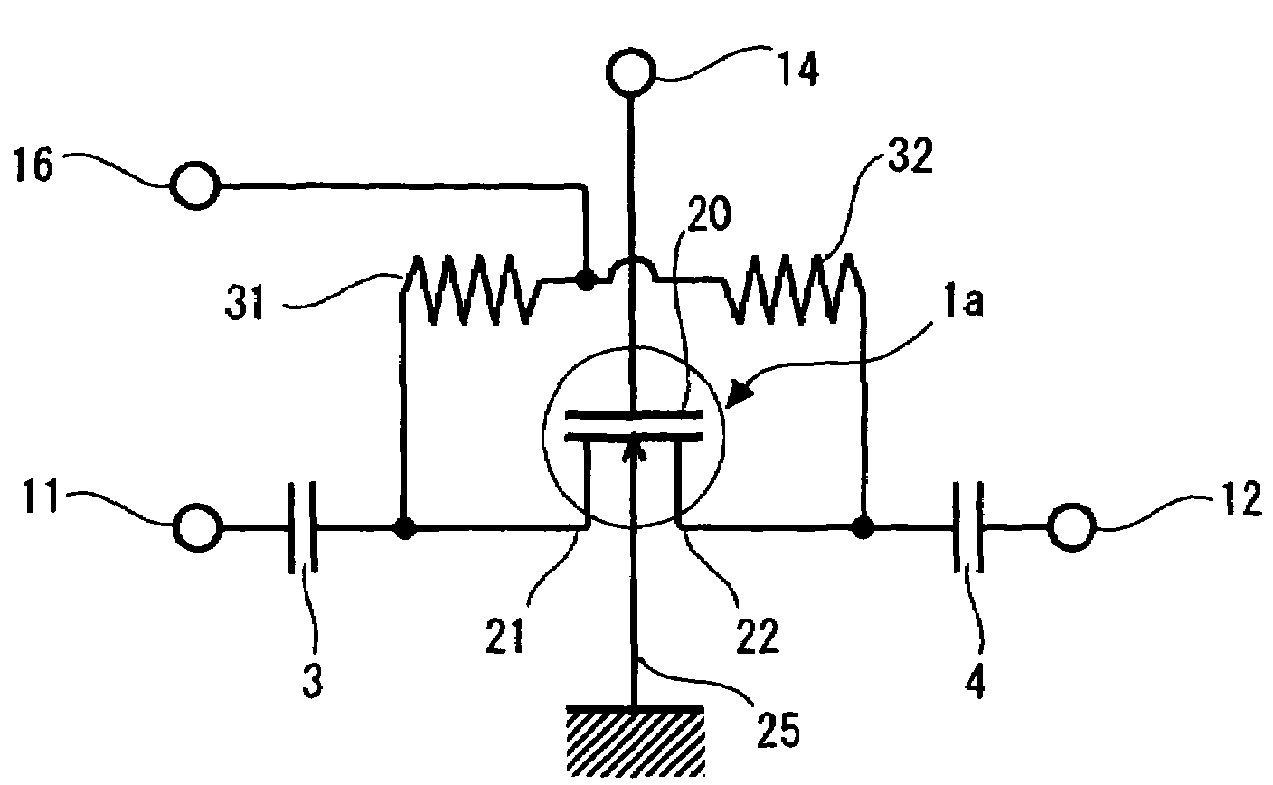
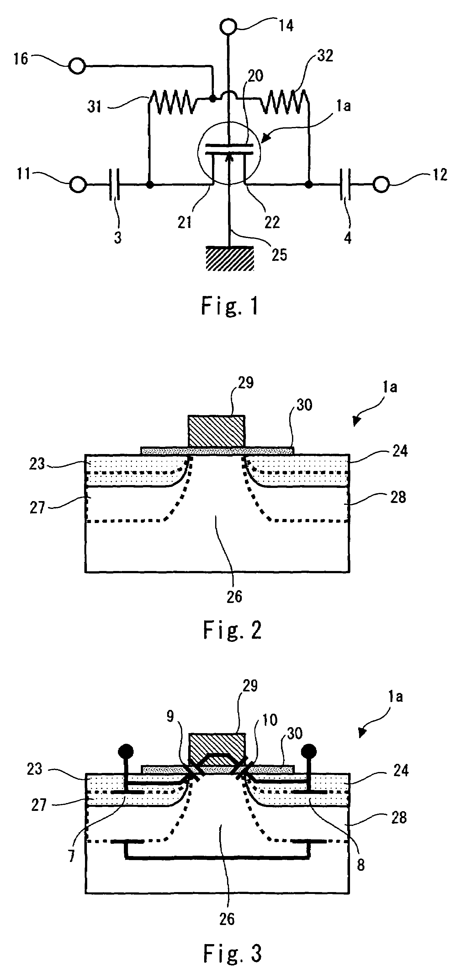
[0031]FIG. 1 is a circuit diagram showing a semiconductor switch according to a first embodiment of the present invention. An RF input terminal 11 and an RF output terminal 12 are connected with a source 21 and a drain 22 of an nMOSFET 1a, respectively. A capacitor 3 for cutting DC components is connected between the source 21 and the RF input terminal 11. Likewise, a capacitor 4 for cutting DC components is connected between the drain 22 and the RF output terminal 12. Further, a backgate 25 of the nMOSFET is grounded, and a gate terminal 20 is connected with a terminal (hereinafter referred to as “control terminal”) 14 for inputting a gate control signal for controlling on / off states of a switch (gate) which is applied to the gate terminal 20.

[0032]In this embodiment, in addition to the above components, a terminal 16 for applying a positive voltage (impedance control signal) to the source 21 and the drain 22 is provided. The terminal 16 is connected with the source 21 and the drai...

second embodiment

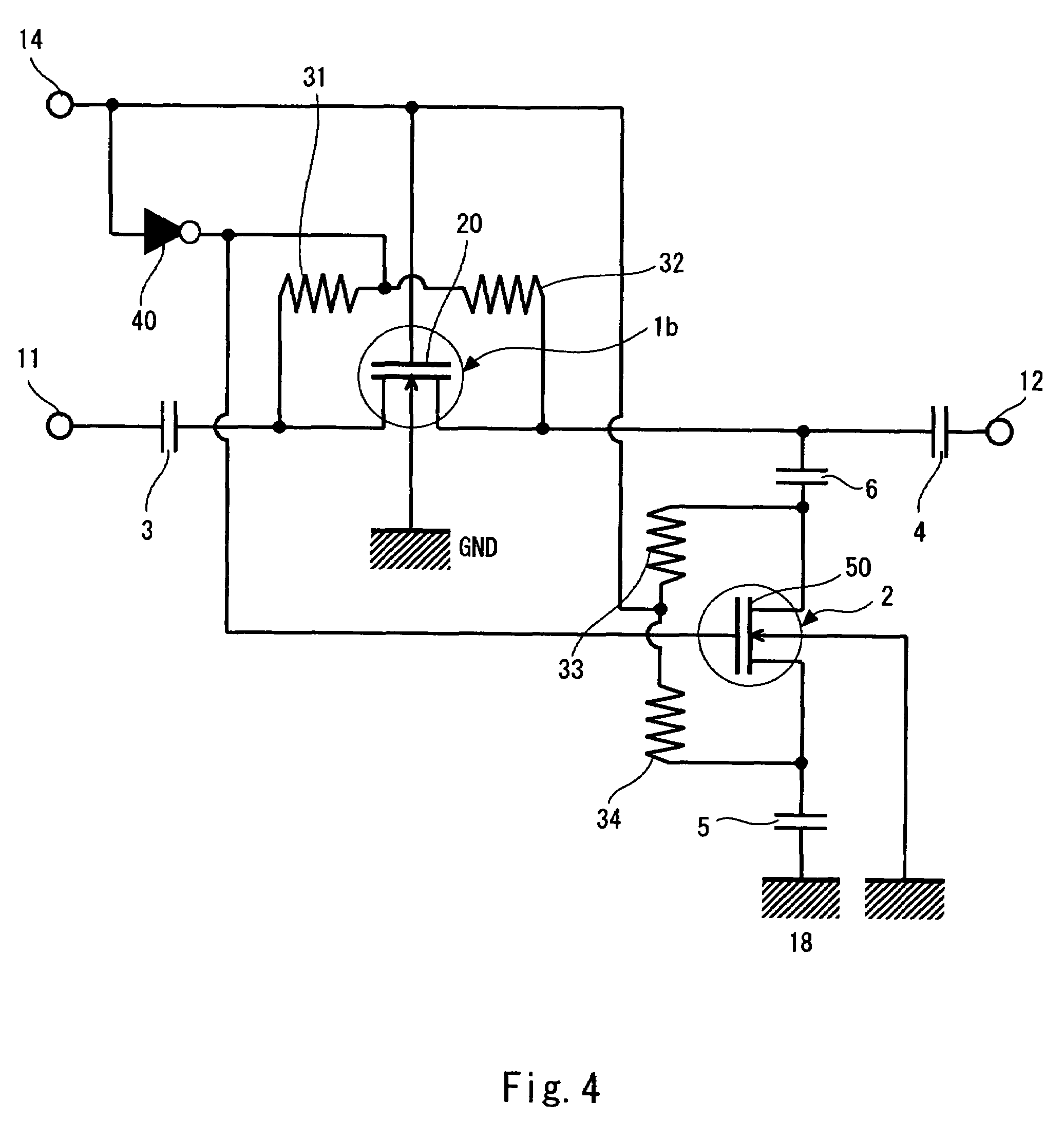
[0040]FIG. 4 is a circuit diagram showing a semiconductor switch according to a second embodiment of the present invention. This embodiment is achieved by applying the present invention to an SPST switch that incorporates a shunt circuit. Incidentally, in this embodiment of FIG. 4, the same components as those of the first embodiment of FIG. 1 are denoted by identical reference numerals, and their detailed description is omitted here.

[0041]The semiconductor switch of this embodiment includes an switching nMOSFET 1b provided between the RF input terminal 11 and the RF output terminal 12 and in addition, a shunt nMOSFET 2 provided between the RF output terminal 12 and the ground terminal 18. A control signal for switching between the switching nMOSFET 1b and the shunt nMOSFET 2 is input from the control terminal 14. Similar to the first embodiment, the control terminal 14 is directly connected with the gate terminal 20 of the switching nMOSFET 1b. Meanwhile, the control terminal 14 is...


PUM


Abstract

A semiconductor switch according to an embodiment of the invention includes resistive members connected with a source and a drain witch are n-type diffusion layers formed in a P-well of an n-type MOSFET. When a gate of the n-type MOFET is turned off, a positive voltage is applied to a node between the resistive members for a reverse bias at a PN junction between the source and the drain, and the well. When the gate is turned on, the node between the resistive members is set to 0 V.

Description

BACKGROUND OF THE INVENTION[0001]1. Field of the Invention[0002]The present invention relates to a semiconductor device suitable for a semiconductor switch for switching an RF signal.[0003]2. Description of Related Art[0004]Existing switches for an RF signal are given below. For example, a PIN diode is used as a single-function switch. Further, a compound semiconductor is mainly used as a multifunctional or high-performance semiconductor switch albeit expensive. It is easy to provide greater functionality to a switch made up of an enhancement type nMOS transistor on an inexpensive Si substrate. However, the switch of this type has a disadvantage in that its performance, especially, isolation characteristic with high frequencies is inferior to that of the compound semiconductor and is required to improve its performance.[0005]FIG. 6 is a circuit diagram showing a conventional switch made up of an enhancement type nMOSFET (hereinafter referred to as nMOSFET). Hereinafter, this semicon...

Claims


Application Information

Patent Timeline
Patent Type & Authority Patents(United States)
IPC IPC(8): H03K17/687
CPCH03K17/6871H03K17/687H03K17/162H03K17/063
Inventor TODA, TETSU
Owner RENESAS ELECTRONICS CORP
Why Eureka
Try Eureka