Microelectronic packages and methods therefor

a technology of microelectronic packages and microelectronic components, applied in the direction of semiconductor devices, semiconductor/solid-state device details, electrical apparatus, etc., can solve the problems of imposing stress on solder, terminals moving relative to the contact, assembly including packages can suffer from stress, etc., to achieve greater height and higher wiring density

Active Publication Date: 2010-05-18
TESSERA INC
View PDF20 Cites 45 Cited by
  • Summary
  • Abstract
  • Description
  • Claims
  • Application Information

AI Technical Summary

Benefits of technology

[0015]In certain preferred embodiments of the present invention, microelectronic packages have dual diameter conductive posts or pins. Each of the conductive posts desirably includes a large diameter conductive base affixed to a flexible dielectric layer or wafer and small diameter conductive tip disposed atop the conductive base. In preferred embodiments, the base and the tip have cylindrical shapes. In more preferred embodiments, the dual diameter conductive post structure includes two concentric cylinders in which the upper cylinder (i.e. the tip) has a greater height than the lower cylinder (i.e. the base). The microelectronic packages preferably include a conductive feature for making electrical connection between the conductive base and a wiring trace on the flexible dielectric layer or wafer. The conductive feature preferably extends between a bottom surface of the conductive base and the wiring trace. Moreover, the conductive feature desirably has a diameter that is smaller than the diameter of the conductive base. The use of the relatively small diameter conductive feature for electrically interconnecting the conductive base with the wiring trace decreases the conductive area of the wiring trace occupied by the conductive base of the post and thereby enables a higher wiring density to be provided on the flexible dielectric layer.
[0016]In preferred embodiments, the larger diameter base insures a good mechanical joint between the base and the dielectric layer. As is well known to those skilled in the art, a peeling stress occurs between the base and the dielectric layer when the post is forced to pitch or roll. The large diameter base helps distribute the peeling stress and thereby improves the mechanical reliability of the interconnection.
[0023]Although the present invention is not limited by any particular theory of operation, it is believed that prior art conductive posts limit the density of wiring traces that may be placed on a flexible dielectric tape or low modulus material on a wafer. For etched pins, this is a consequence of the etching process used for their formation. For formed pins, it is determined by the aspect ratio of holes that can proceed in a thick photo-imageable resist at moderate cost. The posts or pins are grown in the apertures by electroplating or by using other metal deposition methods. The downside of using large diameter bases for the posts is that it limits the surface area that can accommodate a wiring or redistribution trace. In cases where the circuit requires a dense wiring trace, then it is necessary to use a multi-layer approach with vias connecting the buried levels, which increases the cost of manufacture and decreases product reliability. Thus, the present invention seeks to provide high density conductive traces on a flexible dielectric substrate of a package or on low modulus material of a wafer package without compromising the mechanical robustness of the attachment of the conductive posts.
[0039]Assemblies in accordance with preferred embodiments of the present invention facilitate testing of microelectronic elements and packages having non-planar contacts and interfaces, and avoids the need for specialized, expensive test equipment. In preferred methods according to this aspect of the present invention, movement of the bases of the conductive posts contribute to movement of the tips of the posts, allowing the tips to engage opposing contact pads even where the contact pads themselves are not coplanar with one another.

Problems solved by technology

Assemblies including packages can suffer from stresses imposed by differential thermal expansion and contraction of the device and the substrate.
Where the terminals of the package are fixed relative to the chip or other device, such as by using solder, these effects tend to cause the terminals to move relative to the contact pads on the circuit board.
This can impose stresses in the solder that connects the terminals to the contact pads on the circuit board.
Testing of packaged devices poses another formidable problem.
However, it is difficult to make connections by pressing the package against a simple test fixture such as an ordinary circuit board having planar contact pads.
For example, in a BGA package, differences in the diameter of the solder balls attached to the terminals, and non-planarity of the chip carrier, may cause some of the solder balls to lie at different heights.
However, such features add to the cost of the test fixture and, in some cases, introduce some unreliability into the test fixture itself.
This is particularly undesirable because the test fixture, and the engagement of the device with the test fixture, should be more reliable than the packaged devices themselves in order to provide a meaningful test.
This requirement imposes constraints on the electrical characteristics of the signal paths in the test fixture, which further complicates construction of the test fixture.
Additionally, when testing packaged devices having solder balls connected with terminals, solder tends to accumulate on those parts of the test fixture that engage the solder balls.
This accumulation of solder residue can shorten the life of the test fixture and impair its reliability.

Method used


Image

  • Microelectronic packages and methods therefor
  • Microelectronic packages and methods therefor
  • Microelectronic packages and methods therefor

Examples


Embodiment Construction

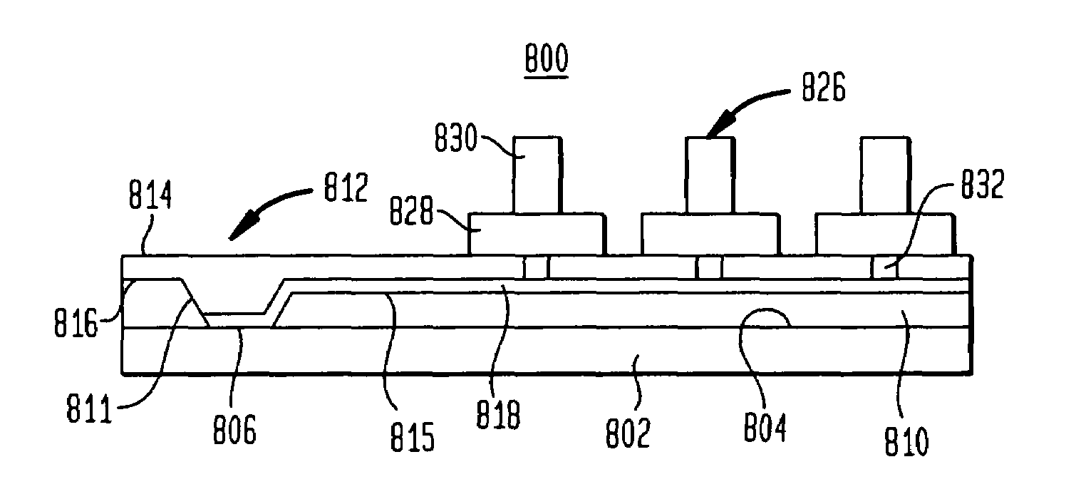
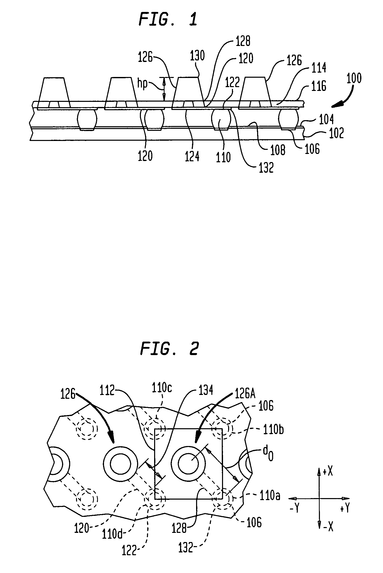
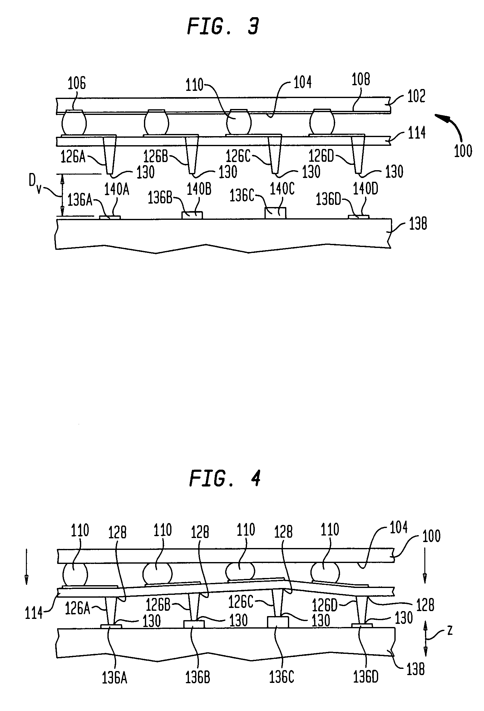
[0066]Referring to FIG. 1, in accordance with one preferred embodiment of the present invention, a microelectronic package 100 includes a microelectronic element, such as a semiconductor chip 102, having a front or contact bearing face 104 and electrical contacts 106 exposed at face 104. A passivation layer 108 may be formed over the contact bearing face 104 with openings at contacts 106.

[0067]The microelectronic package 100 also includes conductive support elements 110 such as solder balls in substantial alignment and electrically interconnected with contacts 106. As best seen in FIG. 2, contacts 106 and support elements 110 are disposed in an array which in this case is a rectilinear grid, having equally spaced columns extending in a first horizontal direction x and equally spaced rows extending in a second horizontal direction y orthogonal to the first horizontal direction. Each contact 106 and support element 110 is disposed at an intersection of a row and a column, so that each...


PUM


Abstract

A microelectronic package includes a microelectronic element having contacts, a flexible substrate spaced from and overlying the microelectronic element and a plurality of conductive posts extending from the flexible substrate and projecting away from the microelectronic element. The conductive posts are electrically interconnected with the microelectronic element. Each conductive post has a conductive base that is in contact with the flexible substrate and a conductive tip that extends from the base, with the base of the conductive post having a larger diameter than the tip of the conductive post. In certain embodiments, the conductive base and the conductive tip have a cylindrical shape.

Description

FIELD OF THE INVENTION[0001]The present invention relates to microelectronic packages and to methods of making and testing microelectronic packages.BACKGROUND OF THE INVENTION[0002]Microelectronic devices such as semiconductor chips typically require many input and output connections to other electronic components. The input and output contacts of a semiconductor chip or other comparable device are generally disposed in grid-like patterns that substantially cover a surface of the device (commonly referred to as an “area array”) or in elongated rows which may extend parallel to and adjacent each edge of the device's front surface, or in the center of the front surface. Typically, devices such as chips must be physically mounted on a substrate such as a printed circuit board, and the contacts of the device must be electrically connected to electrically conductive features of the circuit board.[0003]Semiconductor chips are commonly provided in packages that facilitate handling of the c...

Claims


Application Information

Patent Timeline
Patent Type & Authority Patents(United States)
IPC IPC(8): H01L23/48
CPCH01L23/49811H01L23/4985H01L2224/48091H01L24/48H01L2924/3011H01L2924/00014H01L2224/45014H01L2224/45015H01L2924/207H01L2924/206
Inventor HUMPSTON, GILESGAO, GUILIANHABA, BELGACEM
Owner TESSERA INC
Why Eureka
Try Eureka