Imaging device and method for reading signals from such device

a technology of image sensor and information device, which is applied in the field of image sensor, can solve the problems of difficult to correctly detect optical beacon, large amount of electricity consumed by the system, and inability to incorporate such an image sensor into a small-sized information device, and achieve the effect of increasing the reading speed of pixel signals, high speed, and small area receiving information light within the pixel cell array

Inactive Publication Date: 2010-06-01
JAPAN SCI & TECH CORP +1
View PDF14 Cites 65 Cited by
  • Summary
  • Abstract
  • Description
  • Claims
  • Application Information

AI Technical Summary

Benefits of technology

[0024]In general, the percentage of the area receiving the information light within the pixel cell array is small. Therefore, among all the m×n pixel cells, the number of signal-receiving pixel cells can be regarded to be much smaller than that of the imaging pixel cells. Accordingly, in the signal-reading method according to the first aspect of the present invention, even if the readout of the pixel signal from each signal-receiving pixel cell is repeated more than one time within the second periods of time inserted between each neighboring pair of the fractional time sections of the first period of time for reading pixel signals from all the imaging pixel cells to be used for constructing one frame of image, it will not be necessary to set the effective speed of reading the pixel signals much higher than in the normal signal-reading methods. The repetition count of reading the pixel signal from the same signal-receiving pixel cell during one normal image frame can be determined beforehand according to the frequency of the information light.
[0025]Thus, in the method of reading signals from an imaging device according to the first aspect of the present invention, it is possible to capture normal two-dimensional images and simultaneously extract identification information from an optical beacon or similar information light present within the imaging area without significantly increasing the reading speed of the pixel signals. As a result, the imaging device can operate at high speed while suppressing an increase in the power consumption.
[0026]In a mode of the method of reading signals from an imaging device according to the first aspect of the present invention, the divisional unit of the first period of time is one row of the pixel cell array. In this mode, the readout of pixel signals from the imaging pixel cells in a given row and the readout of pixel signals from one or more signal-receiving pixel cells are alternately performed.
[0027]In another mode of the method of reading signals from an imaging device according to the first aspect of the present invention, the divisional unit of the first period of time corresponds to a fractional section of one row of the pixel cell array. In this mode, the readout of pixel signals from the imaging pixel cells in a fractional section of a given row and the readout of pixel signals from one or more signal-receiving pixel cells are alternately performed.
[0028]The signal-receiving pixel cells from which the pixel signals are to be read during each round of the second periods of time may be those pixel cells located in one row within an information light-receiving area onto which one information light is cast. In this case, the readout of the pixel signals from the imaging pixel cells included in the divisional unit and the readout of the pixel signal from one or more signal-receiving pixel cells located in one row within an information light-receiving area onto which one information light is cast are alternately performed.
[0029]As opposed to the previous case, if the number of the signal-receiving pixel cells among all pixel cells cannot be regarded as much smaller than that of the imaging pixel cells, repeating the readout of pixel signals from all the signal-receiving pixel cells many times will require a higher readout speed. In practice, if the information light-receiving area is large, reducing the number of pixel cells from which the pixel signals are to be read within the aforementioned area will cause no problems because the pixel cells within that area receive the same content of information. Accordingly, if the number of signal-receiving pixel cells within one information light-receiving area is large, it is preferable to reduce the number of pixel cells from which the pixel signal is to be read by skipping a portion of the signal-receiving pixel cells or integrating the pixel signals of a plurality of the signal-receiving pixel cells. This method prevents an unnecessarily large number of pixel signals from being read from the signal-receiving pixel cells, thereby suppressing the increase in the readout speed.

Problems solved by technology

Therefore, it is difficult to correctly detect the optical beacon by generally known methods for reading pixel signals from normal image sensors.
However, this system consumes a considerable amount of electricity; therefore it is necessary to supply a larger amount of current to the circuit components, such as an amplifier for reading the signals, since the operation frequency of the signal-reading circuit increases with the frame frequency.
Incorporating such an image sensor into a small-sized information device is impractical because it will significantly shorten the operating time of the device.
Furthermore, use of an image sensor consuming so much power makes the device difficult to design because the heat-releasing performance must be considered.
Another problem is that the signal-to-noise (S / N) ratio of the readout signal is low.
This is because the readout noise is high due to the high frequency band of the signal-reading circuit while the signal level is low due to the shorter period of time for collecting electric charges.
However, this method is not suitable for creating a high pixel density device because the pixel size is considerably large due to the use of more transistors in one pixel circuit than in a pixel circuit of normal image sensors.
Moreover, another factor impeding the creation of a high pixel density device is that the power consumption per pixel cell is much higher than in conventional cases since electric current must be continually supplied to the amplifier to operate the analogue circuit inside each pixel cell.
This is another factor that impedes the creation of a high pixel density device.

Method used


Image

  • Imaging device and method for reading signals from such device
  • Imaging device and method for reading signals from such device
  • Imaging device and method for reading signals from such device

Examples


Embodiment Construction

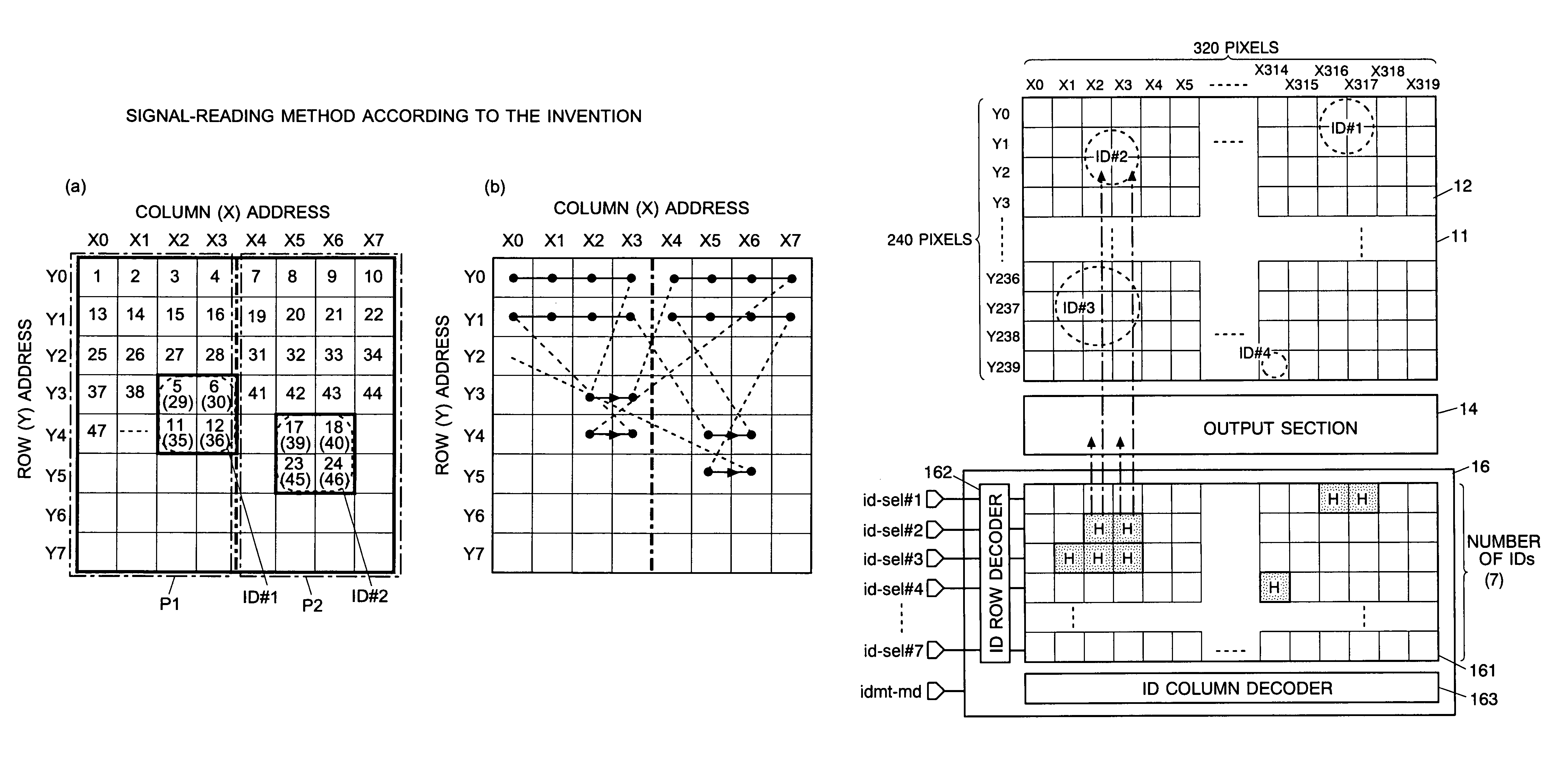
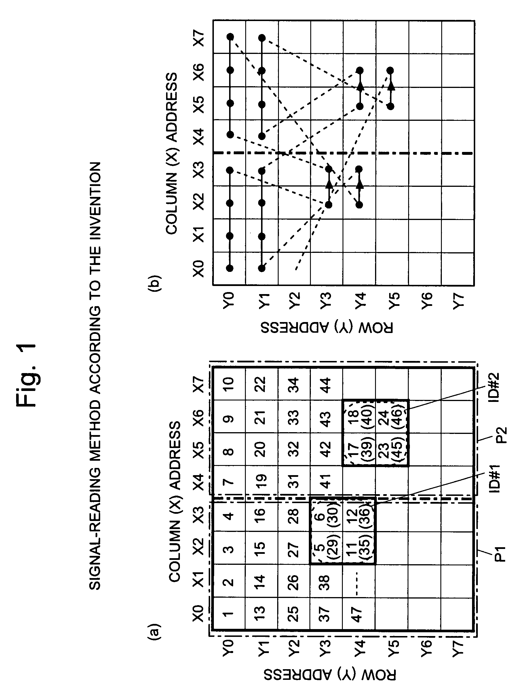
[0052]An example of a free-space optical communication system using an imaging device according to the present invention is described with reference to the attached drawings.

[0053]FIG. 11 is a schematic view of the present free-space optical communication system. The information terminal 1, which is hand-held by a user (not shown), is a mobile phone capable of free-space optical communication. The personal computer 2, digital camera 3 and portable music player 4 are communication nodes capable of sending an ID signal (which corresponds to the identification information in the present invention) through an optical beacon to the information terminal 1. For example, this optical beacon can be created using a light-emitting diode for indicating the on / off state of an electronic device.

[0054]FIG. 13 is a graph showing the frequency spectrums of the signals contained in the light emitted from the optical beacon of each communication node. The pilot signal is a signal that blinks (or chang...


PUM


Abstract

Each pixel cell (12) of an image sensor (10) is made of a 4-Tr structure, in which only one Tr for resetting a column (X) is so added to an ordinary 3-Tr APS as to reset only an arbitrary pixel selectively, thereby to confine the pixel size. When a pixel signal is to be read, the period, for which the pixel signals composing an ordinary image of one frame are read, is finely divided so that the pixel signals of the pixels receiving an ID light for the period are read out bit by bit and repeatedly. At this time, for only the column being read, an electric current is fed to a read amplifier in the pixel cell (12) or a variable gain amplifier in an output unit (14), thereby to suppress the power consumption. As a result, a lower power consumption and a higher pixel formation can be attained in an image pickup device for picking up an image and for acquiring the ID information of a light beacon existing in the image pickup range.

Description

TECHNICAL FIELD[0001]The present invention relates to an imaging device having the functions of capturing an image of an object and receiving an information light blinking or intensity-modulated at a frequency higher than a standard frame frequency within the imaging area. The present invention also relates to a method of reading signals from such an imaging device.BACKGROUND ART[0002]In recent years, a new type of system called the identification (ID) recognition camera system (or ID cam) has been proposed. It includes an optical beacon for emitting a blinking signal containing ID information and other items of information relating to electronic devices and a camera with a high-speed image sensor. For example, a system disclosed in Patent Document 1 captures a series of images with an ID-recognition camera and outputs them as a scene image. Then, it decodes the blinking data of the optical beacon by use of all pixel values to create an ID image. Practical applications of this ID-re...

Claims


Application Information

Patent Timeline
Patent Type & Authority Patents(United States)
IPC IPC(8): H04N3/14H04N5/335
CPCH04N3/155H04N5/335H04N5/23241H04N23/65H04N25/40H04N25/745H04N25/70H04N25/75H04N23/00H04N25/00
Inventor KAGAWA, KEIICHIROMAEDA, YUKIOHTA, JUN
Owner JAPAN SCI & TECH CORP
Why Eureka
Try Eureka