Method and system for reshaping a transistor gate in an integrated circuit to achieve a target objective

a transistor gate and integrated circuit technology, applied in the direction of cad circuit design, program control, instruments, etc., can solve the problems of static power, “useless” power, and today's ic design and manufacturing processes fail to exploit a valuable degree of freedom, so as to reduce leakage power

Inactive Publication Date: 2010-06-01
RPX CORP
View PDF31 Cites 31 Cited by
  • Summary
  • Abstract
  • Description
  • Claims
  • Application Information

AI Technical Summary

Benefits of technology

[0012]Various embodiments of the present invention offer the following advantages. Reshaping the basic shape of transistor channels leads to an Integrated Circuit (IC) that will have reduced leakage power without having a considerable impact on its performance characteristics. In addition the IC can also be designed to improve objectives including with respect to reliability, capacitance, IC parametric yield and manufacturing yield. Various embodiments of the invention are in accordance with existing IC design processes (LOCOS or STI, etc.). The present invention is also capable of being used within the existing IC design cycle, with reshaping performed at the design stage in either the full-custom design or semi-custom design context.

Problems solved by technology

With modern deep-submicron or decananometer-scale IC manufacturing processes, a very serious problem is that of leakage current, and therefore leakage power dissipation.
Static power is also known as “useless” power since it is dissipated without achieving any advancement of useful computations by the circuit.
Therefore, today's IC design and manufacturing processes fail to exploit a valuable degree of freedom, whereby not only the length and width but more generally, the shape of the transistor channel can be optimized to achieve a target objective with respect to performance, power, reliability, manufacturing yield, and other metrics.
Due to this failing, today's IC design and manufacturing processes suffer unnecessary loss of performance, power, reliability, and parametric yield in manufactured ICs.

Method used


Image

  • Method and system for reshaping a transistor gate in an integrated circuit to achieve a target objective
  • Method and system for reshaping a transistor gate in an integrated circuit to achieve a target objective
  • Method and system for reshaping a transistor gate in an integrated circuit to achieve a target objective

Examples


Embodiment Construction

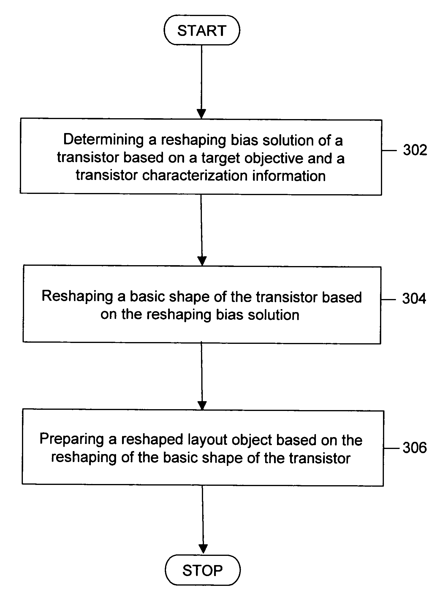
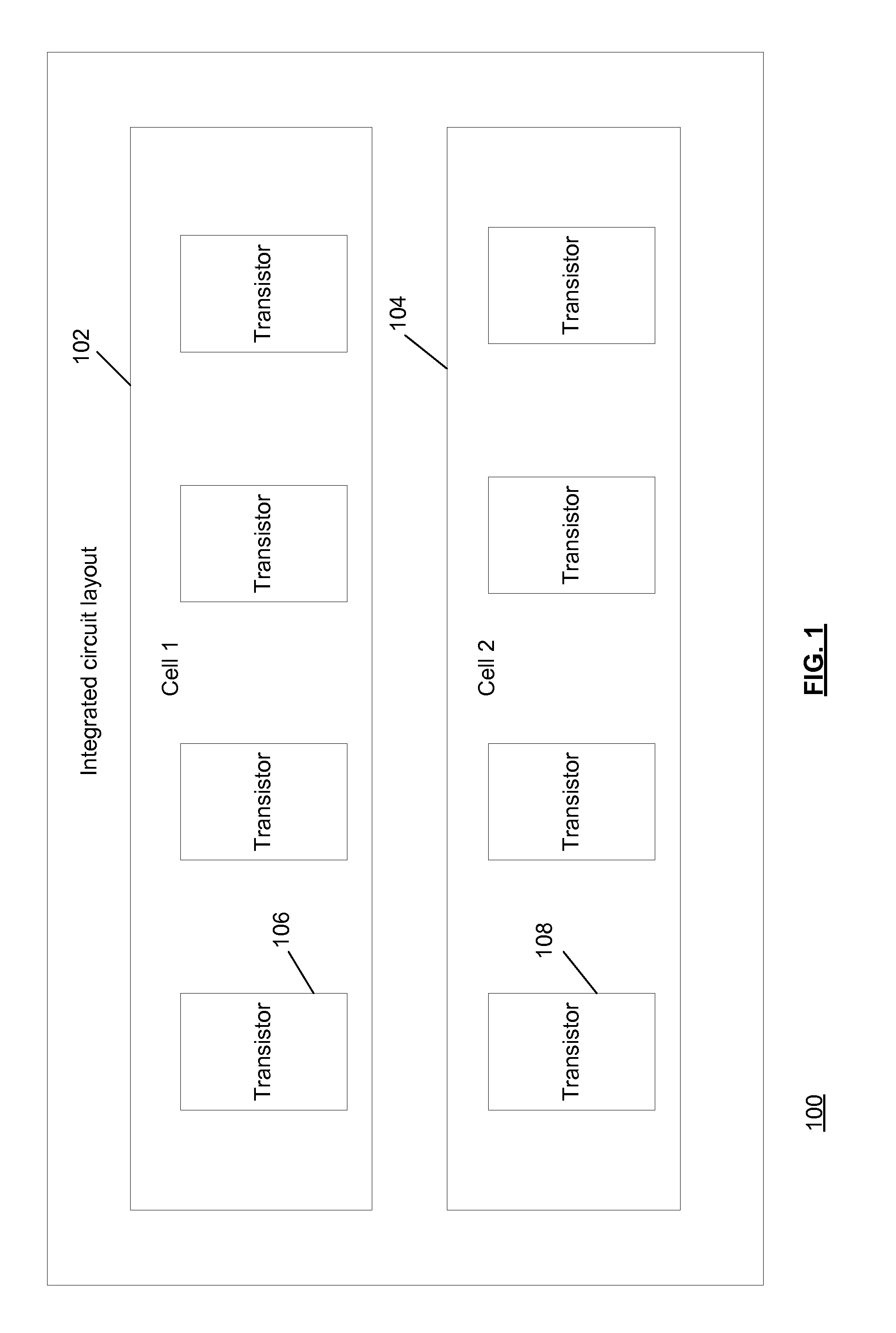
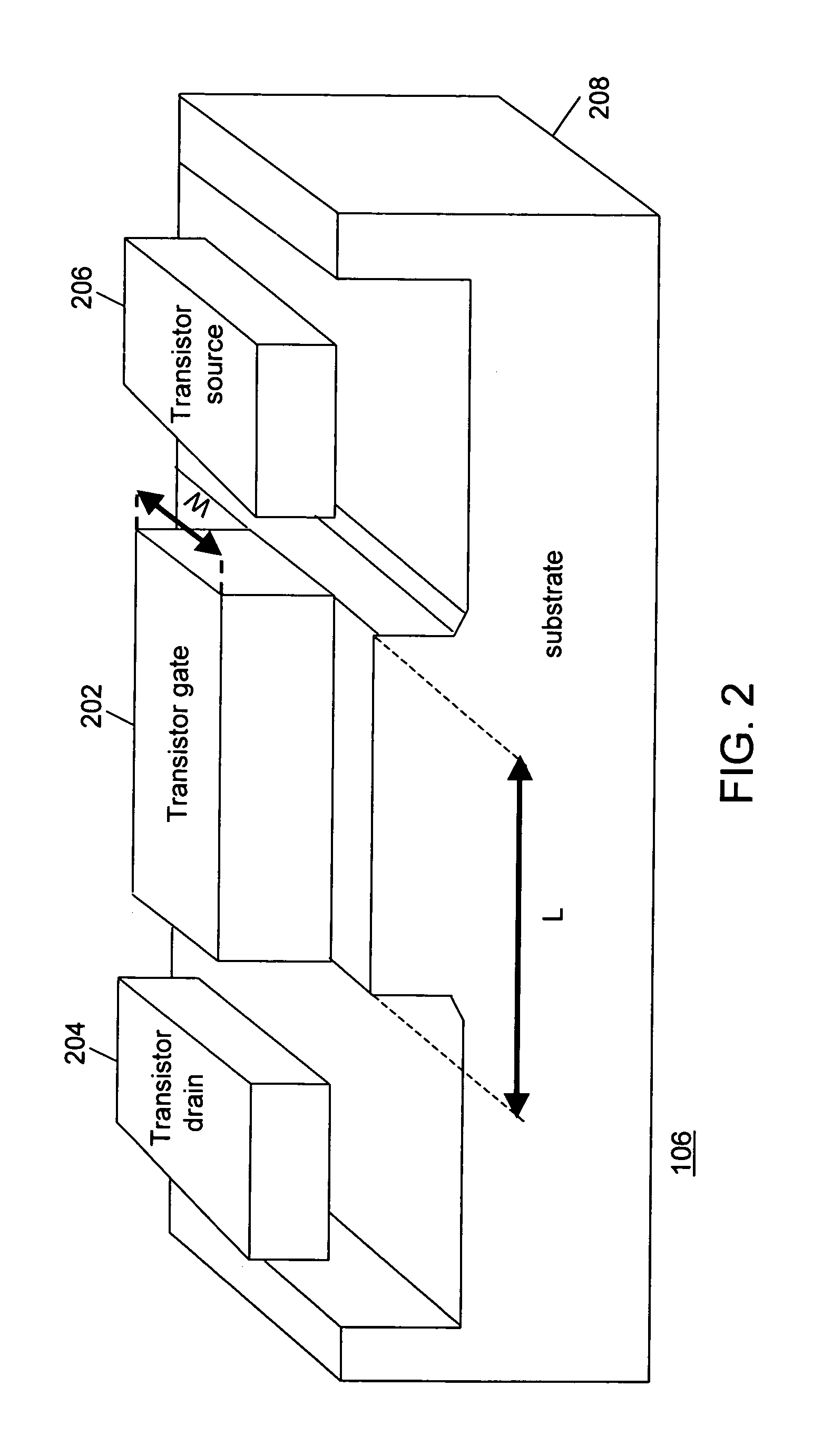
[0027]The present invention relates to a method and system for designing an integrated circuit (IC), which includes a plurality of cells. Each of the plurality of cells includes a plurality of transistors. The present invention provides for a method to achieve one or more target objectives in the IC. The target objectives include, but are not limited to, a performance objective, a leakage objective, capacitance, reliability, a manufacturing yield, and an IC parametric yield. Each of the target objectives includes the target values of a plurality of transistor metrics. For example, the performance objective of a transistor is characterized by the drive current (Ion) of that transistor, and the leakage objective of a transistor is characterized by the leakage current (Ioff) of that transistor. Similarly, capacitance is characterized by a plurality of capacitances, such as the transistor gate to transistor drain capacitance, the transistor gate to transistor channel capacitance, and th...


PUM


Abstract

The present invention provides a method and system for designing an integrated circuit (IC). The IC comprises a plurality of cells, and each of the cells comprises a plurality of transistors. The method achieves a target objective of a transistor, of a cell, or of part of or the entire IC. The method of designing the IC includes reshaping a basic shape of the transistor. The method includes determining a reshaping bias solution of the transistor. The method further includes modifying the basic shape of the transistor channel, based on the reshaping bias solution, and preparing a reshaped layout design.

Description

[0001]This application claims priority of U.S. provisional application Ser. No. 60 / 666,385 filed on Mar. 30, 2005.BACKGROUND OF THE INVENTION[0002]1. Field of the Invention[0003]This invention relates in general to the design of integrated circuits (ICs) and in particular to designing IC layouts.[0004]2. Description of the Related Art[0005]In the design and manufacture of modem Integrated Circuits (ICs), a number of advanced technologies are applied in concert to achieve uniformity and fidelity of all the patterned IC features, including transistors. Such advanced technologies span computer-aided design tools, photomask design tools and fabrication equipment, as well as lithography tools in the foundry. In all of these technologies, the simulation model of the transistor is based on idealized transistor channel widths and lengths. The transistor channel is modeled for simulation purposes as a rectangle. Further, the physical realization of the transistor channel, as represented in a...

Claims


Application Information

Patent Timeline
Patent Type & Authority Patents(United States)
IPC IPC(8): G06F17/50
CPCG06F17/5068G06F30/39
Inventor GUPTA, PUNEETKAHNG, ANDREWREED, DAVE
Owner RPX CORP
Why Eureka
Try Eureka