Microstructure and manufacturing method thereof and microelectromechanical system

a manufacturing method and microelectromechanical technology, applied in the field of microelectromechanical system, microelectromechanical system, electrical apparatus, etc., can solve the problems of immediate breakage of structure, unsuitability of structure formed using tungsten film or molybdenum film, etc., to achieve excellent resistance and excellent reliability.

Inactive Publication Date: 2010-06-08
SEMICON ENERGY LAB CO LTD
View PDF48 Cites 6 Cited by
  • Summary
  • Abstract
  • Description
  • Claims
  • Application Information

AI Technical Summary

Benefits of technology

[0008]However, when a metal film such as a tungsten film and a molybdenum film is formed by a sputtering method, such metal is easily grown in a needle-like crystal in a direction perpendicular to a substrate.
[0012]In view of the problems described above, an object of the present invention is to improve strength against breakage of a metal layer such as a molybdenum film or a tungsten film which is used as a microstructure of a microelectromechanical system.
[0015]In this manner, a metal layer having a plate-like crystal can be obtained. In other words, the metal layer in which a needle-like crystal is reduced or removed can be obtained. Therefore, a microelectromechanical system which is strong against breakage can be obtained by using this metal layer as a structural layer of the microstructure.
[0024]In this manner, the first conductive film having a plate-like crystal can be obtained. That is, a needle-like crystal of the first conductive film can be reduced or removed. Therefore, an FBAR filter which is strong against breakage can be obtained by using the first conductive film as a structural layer of a microstructure.
[0036]According to the present invention, a needle-like crystal in a structural layer is reduced or removed by laser irradiation, so that a microstructure which is strong against breakage can be obtained. For example, when a structural layer oscillating up and down is irradiated with a laser beam, since crystal grain boundaries which exist in the same direction as a direction to which stress applies are reduced or removed to become a plate-like crystal, the structural layer is hard to be destroyed. By using a microstructure including this structural layer, a microelectromechanical system which is excellent in a resistance property and excellent in reliability can be provided. Note that a microstructure according to the present invention can be used in various fields related to a MEMS, and for example, the microstructure can be used as a sensor such as an acoustic wave sensor, a position sensor, a magnetic sensor, a chemical sensor, a gas sensor, or a humidity sensor. In addition, the microstructure can be applied to a resonator, a micro gear, a generator or the like.

Problems solved by technology

Therefore, when a structure formed using a tungsten film or a molybdenum film by a sputtering method as a movable portion such as a MEMS switch is used as it is, the structure is immediately broken; therefore, the structure formed using the tungsten film or the molybdenum film is unsuitable for a structure.
Therefore, in the case where the metal layer is formed over a glass substrate or a plastic substrate by a sputtering method, since the metal layer is required to be formed at a relatively low temperature, a problem of breakage of a structure becomes apparent when such a metal layer is used as the structure.

Method used


Image

  • Microstructure and manufacturing method thereof and microelectromechanical system
  • Microstructure and manufacturing method thereof and microelectromechanical system
  • Microstructure and manufacturing method thereof and microelectromechanical system

Examples


embodiment mode 1

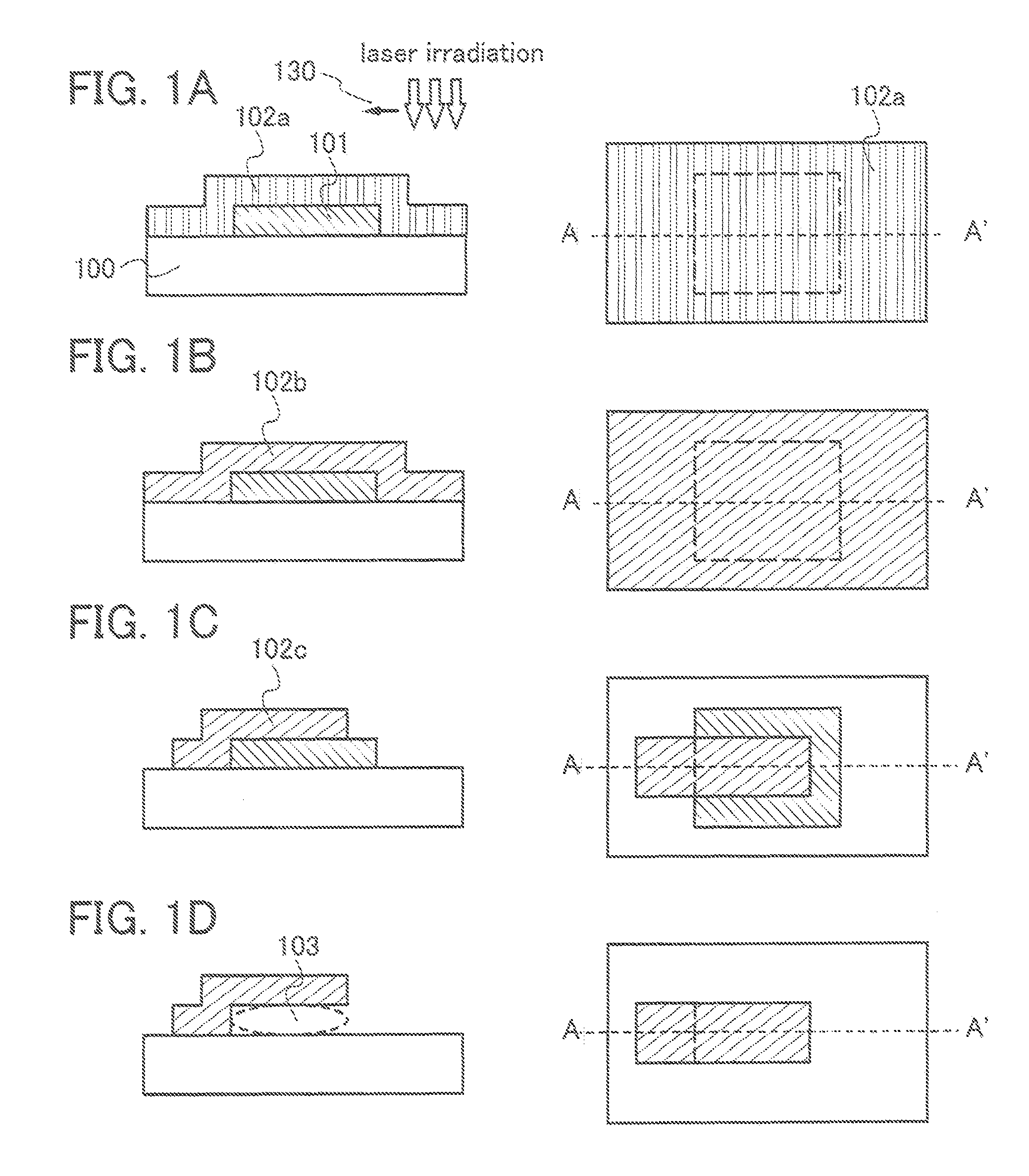
[0050]In this embodiment mode, a manufacturing method of a microstructure in which a crystalline state of a structural layer is changed by laser irradiation is described.

[0051]A substrate 100 is prepared as shown in FIG. 1A. Note that respective cross-sectional views shown on the left side of FIGS. 1A to 1D correspond to dotted lines A-A′ of top plan views shown on the right side respectively.

[0052]A quartz substrate, a glass substrate, a plastic substrate, a silicon substrate, or the like can be used as the substrate 100. For example, by forming a microstructure over a plastic substrate, a device having a thin, lightweight, and highly flexible microstructure can be formed. In addition, by thinning a quartz substrate, a glass substrate, or a silicon substrate by polishing, a thin microstructure can be formed.

[0053]Next, a sacrificial layer 101 is formed over the substrate 100. Note that the sacrificial layer means a layer which is selectively removed in a later step. Therefore, the ...

embodiment mode 2

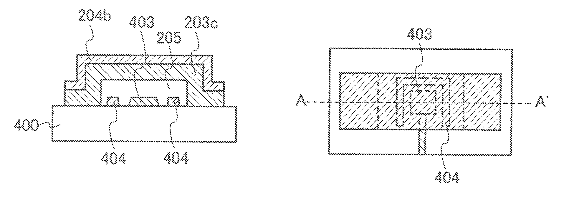
[0076]In this embodiment mode, a bridge-type microstructure switch to which a manufacturing method according to the present invention is applied is described with reference to FIGS. 3A to 3F. Note that in this embodiment mode, a microstructure can be driven by electrostatic attraction. Note that cross-sectional views on the left side of FIGS. 3A to 3F correspond to dotted lines A-A′ of top plan views of the right side.

[0077]First, a first conductive layer 201 functioning as a lower electrode is formed over a substrate 200. The first conductive layer 201 is formed using a metal material selected from W, Mo, Ti, Ta, Pt or Ag, an alloy containing the metal material as its main component, or a material having conductivity by a sputtering method, for example, and etched into a predetermined shape. The first conductive layer 201 can be used as a common electrode, a control electrode or the like.

[0078]A sacrificial layer 202 is processed into a predetermined shape by photolithography over ...

embodiment mode 3

[0093]In this embodiment mode, a Film Bulk Acoustic Resonator (FBAR) filter to which a manufacturing method according to the present invention is applied is described with reference to FIGS. 5A to 5D.

[0094]An FBAR is a kind of an RF-MEMS device formed using a semiconductor process technique, and a filter body is constituted by a piezoelectric thin film and an electrode provided above and below the piezoelectric thin film. Frequency is determined by mechanical vibration of this portion. The FBAR filter according to this embodiment mode can be operated at a high frequency band above 10 GHz and also be applied to a mobile phone.

[0095]A sacrificial layer 301 is formed over a substrate 300 as shown in FIG. 5A. A quartz substrate, a glass substrate, a plastic substrate, a silicon substrate or the like can be used as the substrate 300. For example, by forming a microstructure over a plastic substrate, an FBAR filter which is light, thin and highly flexible can be formed. In addition, by th...


PUM

PropertyMeasurementUnit
melting pointaaaaaaaaaa
thicknessaaaaaaaaaa

Abstract

An object is to provide a microstructure in which shear stress of a structural layer is increased, a manufacturing method thereof, and a microelectromechanical system. A sacrificial layer is formed over a substrate. A metal film is formed over the sacrificial layer. The metal film is irradiated with a laser beam. Needle-like crystals of the metal film are reduced or eliminated. The metal film is etched and processed into a predetermined shape to form a metal layer. Then, the sacrificial layer is removed. Accordingly, a microelectromechanical system which is excellent in reliability and in which a resistance property to breakage of a movable portion of the microstructure is improved can be provided.

Description

BACKGROUND OF THE INVENTION[0001]1. Field of the Invention[0002]The present invention relates to a microstructure irradiated with a laser beam, a manufacturing method thereof, and a microelectromechanical system.[0003]2. Description of the Related Art[0004]In recent years, a device using a microelectromechanical system which is so-called micro electro mechanical systems (MEMS) such as a micro switch, an actuator, a pressure sensor, an acceleration sensor, or the like has been applied in various fields.[0005]A structural layer is formed over a sacrificial layer, and then the structural layer is formed spatially in a space by removing the sacrificial layer by etching, so that a MEMS is driven.[0006]Metal such as tungsten (W) or molybdenum (Mo) is used as such a structural layer which is used as an operation portion of a MEMS (e.g., see Reference 1: Japanese Published Patent Application No. 2005-210614). Tungsten and molybdenum are both group 6 elements, and have a property of high mec...

Claims


Application Information

Patent Timeline
Patent Type & Authority Patents(United States)
IPC IPC(8): H01L21/20
CPCB81C1/00682B81B2203/0118
Inventor YAMAGUCHI, MAYUMIIZUMI, KONAMISHIRAISHI, KOJIRO
Owner SEMICON ENERGY LAB CO LTD
Why Eureka
Try Eureka