Multilayer circuit board and manufacturing method thereof

a multi-layer circuit board and manufacturing method technology, applied in the direction of printed circuit aspects, lithographic masks, etching metal masks, etc., can solve the problems of increasing the cost, limiting the application of multi-layer circuit boards, and the insulating film in such laminated boards tends to bend or wrinkle, and achieves low electrical connection resistance, high reliability, and easy positioning

Inactive Publication Date: 2010-06-15
PANASONIC CORP
View PDF15 Cites 16 Cited by
  • Summary
  • Abstract
  • Description
  • Claims
  • Application Information

AI Technical Summary

Benefits of technology

[0021]In view of the problems in the conventional techniques, an object of the present invention is to provide a multilayer circuit board having low electrical connection resistance and high reliability, and its manufacturing method which makes easy the positioning between lands and via holes and reduces mounting failures resulting from reduced line width of fine etched wiring patterns.
[0023]With this structure, because of the holes in the conductor layers (lands) are connected to and matched in position with the via holes, the multilayer circuit board has reduced electrical connection resistance and improved reliability.
[0026]The wiring pattern of the conductor layer is preferably embedded in the insulating material, so that conductive fillers in the conductive paste make tight contact with each other and with the copper lands to achieve lower electrical connection resistance.
[0029]The wiring pattern is formed by etching on the releasable carrier and transferred onto the insulating material. This way, the line bottom of the wiring patterns will be on the front side, whereby mounting failures that result from reduced line width of etched wiring patterns are reduced.

Problems solved by technology

The key issue of multilayer circuit boards is how to establish electrical connection between layers to form three-dimensional circuits.
While the plating method has the advantage of accomplishing a low resistance connection between fine circuits, it involves complex processes and a large number of process steps, which increases the cost and poses a limitation to the application of multilayer circuit boards.
Insulating films in such laminated boards tend to bend or wrinkle, because of which dimension stability is becoming hard to achieve.
The positioning between via holes and lands is especially difficult, as lands in high density wiring have a very small diameter.
If the via hole is offset from the land, the electrical connection resistance increases or varies, which will lead to a problem.
Such reduced pattern line width will make it difficult to mount semiconductor chips by wire bonding of gold wires, because the bonding points will easily be displaced from the pattern lines.
Multilayer circuit boards using conductive paste had the drawbacks that the electric resistance of the conductive paste was high and contact resistance between the paste and copper foil circuit was unstable, but various improvements have been made.
With the above-described conventional board in which lands protrude from the insulating layer on the front surface of the board, the conductive paste could not be compressed enough to achieve the effect of reducing electrical connection resistance.

Method used


Image

  • Multilayer circuit board and manufacturing method thereof
  • Multilayer circuit board and manufacturing method thereof
  • Multilayer circuit board and manufacturing method thereof

Examples


first embodiment

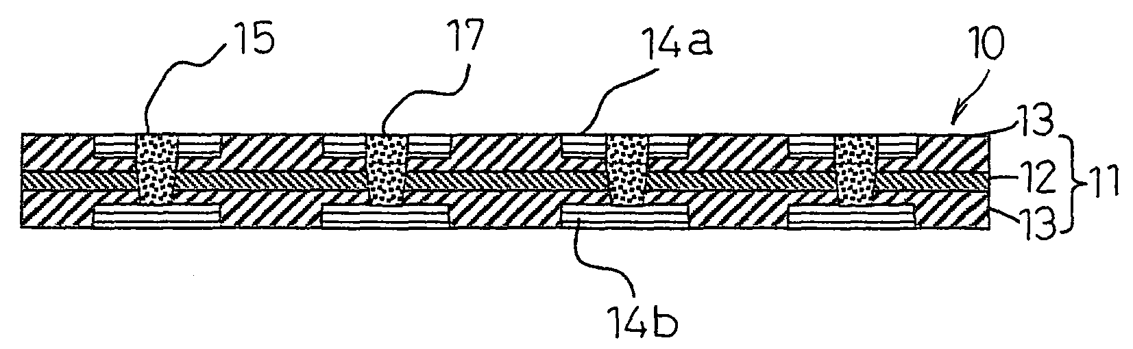
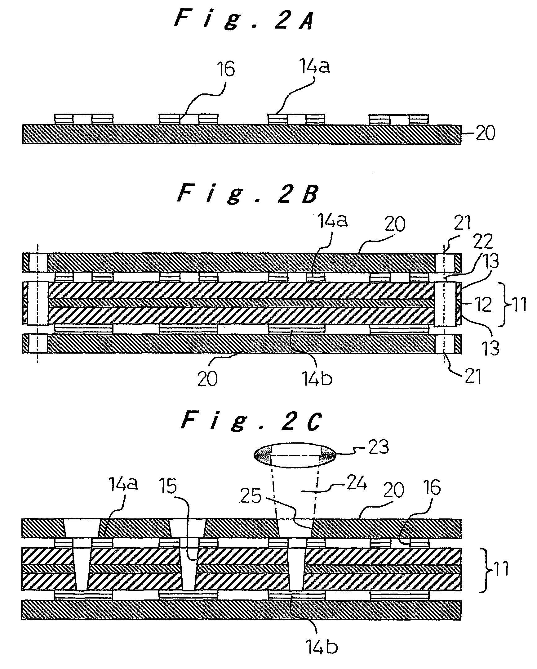
[0042]A first embodiment of the invention is described with reference to FIG. 1 to FIG. 3C. Referring to FIG. 1, a core board (first wiring board) 10, which is a multilayer circuit board with two conductor layers, consists of an insulating material 11 formed by an insulating film 12 and adhesive layers 13 on both sides of the film 12. Conductor layers of copper foil or the like (lands and wiring patterns) 14a and 14b are embedded in the adhesive layers 13. The conductor layer 14a on one side has holes 16 communicating with via holes 15 for the interconnection between both the conductor layers 14a and 14b. The via holes 15 and the holes 16 are filled with conductive paste 17.

[0043]The insulating material 11 is made of a 0.0125 mm thick polyimide film 12 and polyimide-based adhesive 13 applied on both sides of the film 12 in a thickness of 0.01 mm to form the three-layer structure.

[0044]The via holes 15 in the core board 10 are formed by a laser beam irradiated from the side of the co...

second embodiment

[0060]A second embodiment of the invention is described next with reference to FIG. 4 to FIG. 5C. The multilayer circuit board of this embodiment consists of the core board (first wiring board) of the previous embodiment and two other conductor layers (second wiring board) to form a four-layer structure. Same elements as those in the first embodiment are given the same reference numerals and will not be described again.

[0061]In FIG. 4, the reference numeral 10 denotes the same core board (first wiring board) as in the previous embodiment. Two other boards (second wiring board) 30 are laminated on both sides of the core board 10. Each laminated board 30 is an insulating material 11 consisting of an insulating film 12 and adhesive layers 13 on both sides of the film. A conductor layer 14c of copper foil or the like including lands and wiring patterns is embedded in one adhesive layer. The conductor layer 14c is provided with holes 16 that connect to via holes 15 for interconnection. T...

third embodiment

[0067]A third embodiment of the invention is described next with reference to FIG. 6. The multilayer circuit board of this embodiment consists of the core board (first wiring board) of the first embodiment and another conductor layers on both sides of the core board to form a four-layer structure. The difference from the second embodiment is that the laminated boards (second wiring boards) 31 consist of an insulating film 12 and an adhesive layer 13 on only one side of the film. Other features are the same as the second embodiment and will not be described again. Also, the manufacturing method of this embodiment is substantially the same as that of the second embodiment, except that the conductor layers 14a and 14b of the core board 10 are a 0.009 mm thick copper foil, and will not be described again.

[0068]The multilayer circuit board with four conductor layers shown in FIG. 6 thus produced has low electrical connection resistance and improved reliability, and the above manufacturin...


PUM

PropertyMeasurementUnit
thicknessaaaaaaaaaa
thicknessaaaaaaaaaa
diameteraaaaaaaaaa

Abstract

Holes having the same diameter as via holes are formed in predetermined positions in advance when forming wiring patterns on releasable carriers. The carriers with the wiring patterns are bonded on an insulating material, and a laser beam is irradiated from the side of the carrier using the holes in the wiring pattern as a laser mask to form via holes in the insulating material. The via holes and the holes in the carrier are then filled with a conductive paste. With the holes in the carrier that are matched in position with the via holes, lands in the conductor layers are precisely positioned relative to the via holes. A multilayer circuit board thus produced has lower electrical connection resistance and excellent mountability with improved performances. Also a manufacturing method thereof is achieved.

Description

[0001]The present disclosure relates to subject matter contained in priority Japanese Patent Application No. 2005-018651 filled on Jan. 26, 2005, the contents of which is herein expressly incorporated by reference in its entirety.BACKGROUND OF THE INVENTION[0002]1. Field of the Invention[0003]The present invention relates to a multilayer circuit board and a manufacturing method thereof, and more particularly to a multilayer circuit board with via holes filled with conductive paste for providing interconnection between layers and a manufacturing method thereof.[0004]2. Description of the Related Art[0005]As electronic equipment becomes lighter, thinner, and smaller, the size and terminal pitch of semiconductor chips and electronic components are reduced, and accordingly printed circuit boards and package boards become more densely packed. Information technology equipment now requires shorter wiring distances between chips as the signal frequency has increased. Multilayer printed circ...

Claims


Application Information

Patent Timeline
Patent Type & Authority Patents(United States)
IPC IPC(8): H01R12/04H05K1/11
CPCH05K3/20H05K3/4069H05K3/4614H05K3/0035H05K3/4652H05K3/4658Y10T29/49165H05K2201/0394H05K2201/0969H05K2203/0278H05K2203/0554H05K2203/1453H05K2201/0376
Inventor KOYAMA, MASAYOSHIHAYASHI, YOSHITAKEOTANI, KAZUO
Owner PANASONIC CORP
Why Eureka
Try Eureka