Method for manufacturing electrode plate having transparent type or reflective type multi-layered conductive film

a technology of conductive film and electrode plate, which is applied in the field of electrode plate, can solve the problems of reducing the reflectance of aluminum due to the lowering of the reflectance of aluminum, the inability to fully utilize the portability of the liquid crystal display device originally, and the inability to fully utilize the portability of the liquid crystal display device, etc., and achieves excellent optical characteristics (transmittance, reflectance), good patterning configuration, and low electrical connection resistance

Inactive Publication Date: 2001-10-04
FUKUYOSHI KENZO +2
View PDF0 Cites 30 Cited by
  • Summary
  • Abstract
  • Description
  • Claims
  • Application Information

AI Technical Summary

Benefits of technology

[0017] This-invention is made to solve the above problem and an object of this invention is to provide an electrode plate including a transmission type or reflective type conductive film and having an excellent optical characteristic (transmittance, reflectance), low electrical connection resistance, good patterning configuration and high reliability.

Problems solved by technology

In the transmission type liquid crystal display device, since the power consumption by the back light lamp is large and thus the service life is short in the case of battery driving, the portability which the liquid crystal display device originally has cannot be fully utilized.
This is because aluminum is a metal having a large reflectance of light in the visible region, but recently, it is proposed to use silver as a material of the reflection film from the viewpoint of enhancement of the reflectance and a problem that a lowering in the reflectance of aluminum due to contact with the liquid crystal or glass substrate occurs.
First, the adhearability thereof to the substrate of a material such as glass or plastic is low and it is easily separated from the substrate when it is formed on the substrate as a thin silver film.
At this time, since the adhesion between the SiO.sub.2 film and the silver-series thin film is poor, it is necessary to form an adhesion layer formed of a thin oxide film between the SiO.sub.2 film and the silver-series thin film.
Therefore, the manufacturing process becomes complicated and the manufacturing cost is increased.
Secondly, a silver-series thin film formed of highly pure silver on the substrate tends to aggregate and become opaque by the influence of heat and oxygen and the reflectance of light tends to be lowered.
Thirdly, in a case where the thin silver film is exposed and made in direct contact with the outside air, silver sulfide or silver oxide is formed on the surface of the thin silver film and the thin silver film becomes discolored and the reflectance thereof is lowered.
However, the above proposal has the following problem.
When the three-layered conductive film of the above proposal is patterned by the photolithography process by use of an etching solution, contact corrosion due to contact between different types of metals occurs, damage due to the etching process (particularly, damage to the interface between the thin silver film and the oxide film) is large, and particularly, the upper side oxide layer may be easily separated.
But in this case, the electrical connection resistance of the conductive film becomes high and it is not desirable as the conductive film.
Further, as described before, since damage to the interface between the thin silver film and the oxide film occurs, the reliability such as humidity resistance is greatly lowered and it does not reach the practical level.

Method used


Image

  • Method for manufacturing electrode plate having transparent type or reflective type multi-layered conductive film
  • Method for manufacturing electrode plate having transparent type or reflective type multi-layered conductive film

Examples


first embodiment

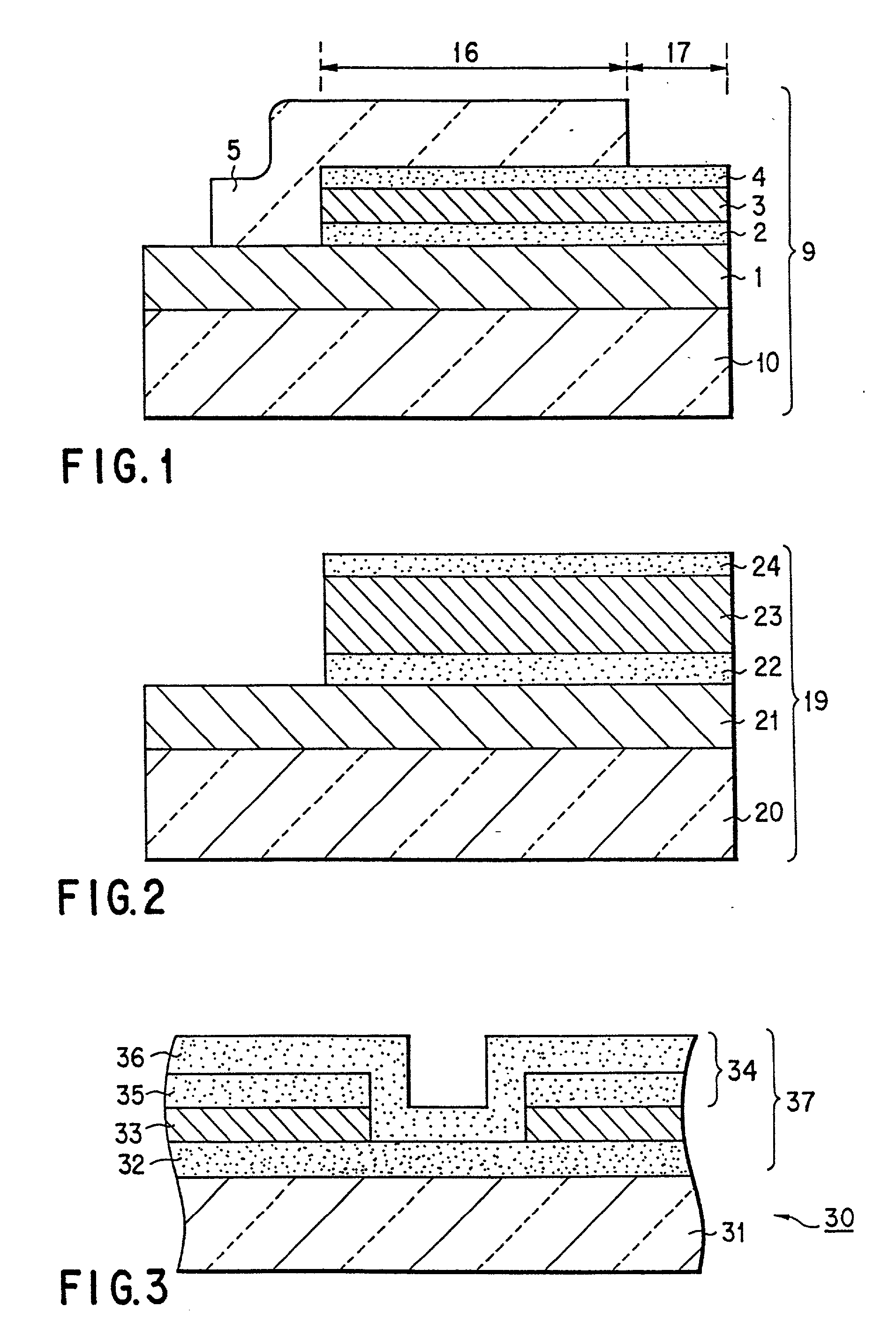
[0063] FIG. 1 is a view showing the schematic structure of an electrode plate according to a first embodiment of this invention.

[0064] In FIG. 1, the main portion of an electrode plate 9 according to the first embodiment is constructed by a glass substrate 10 (made by Corning Co. 1737 material) with a thickness of 0.7 mm and an underlaid layer 1 with a thickness of 29 nm, a lower side amorphous oxide layer 2 with a thickness of 10 nm (as will be seen later, the lower side amorphous oxide function as a lower side anchoring layer), a silver-based layer 3 with a thickness of 15 nm, an upper side amorphous oxide layer 4 with a thickness of 10 nm (as will be seen later, the upper side amorphous oxide function as an upper side anchoring layer) and a protection layer 5 with a thickness of 29 nm which are sequentially laminated on the glass substrate 10. The lower side amorphous oxide layer 2, thin silver-based layer 3, and upper side amorphous oxide layer 4 form a multi-layered conductive ...

second embodiment

[0097] FIG. 2 is a view showing the schematic structure of an electrode plate according to a second embodiment of this invention.

[0098] In FIG. 2, the main portion of an electrode plate 19 is formed by forming an underlaid layer 21 formed of SiO.sub.2 with a film thickness of 40 nm on a glass substrate 20 (made by NIHON ITAGARASU KABUSHIKI KAISHA, H coat product) with a film thickness of 0.7 mm and then sequentially laminating a lower side amorphous oxide layer 22 (a lower side anchoring layer) with a film thickness of 20 nm, a silver-based layer 23 with a film thickness of 150 nm, and an upper side amorphous oxide layer 24 (an upper side anchoring layer) with a film thickness of 7 nm. The lower side amorphous oxide layer 22, thin silver-series thin film 23, and upper side amorphous oxide layer 24 form a multi-layered conductive film.

[0099] The electrode plate 19 according to the second embodiment is a reflective type electrode plate since the film thickness of the silver-based laye...

third embodiment

[0125] As shown in FIG. 3, an electrode plate 30 according to a third embodiment of this invention has a laminated film 37 formed on a glass substrate 31 having an SiO.sub.2 (silicon oxide) layer coated on the surface thereof and having an alkali barrier function. The laminated film 37 is formed of a lower side amorphous oxide layer 32, silver-based layer 33 and upper side oxide layer 34 and the upper side oxide layer 34 is a multi-layered layer having a first amorphous oxide layer 35 (anchoring layer) and a second amorphous oxide layer 36 laminated on the first amorphous oxide layer 35. The film thickness of the lower side amorphous oxide layer 32 is set to 25 nm, the film thickness of the silver-based layer 33 is set to 15 nm, the film thickness of the amorphous oxide layer 35 is set to 10 nm, and the film thickness of the second amorphous oxide layer 36 is set to 30 nm. The lower side amorphous oxide layer 32, silver-based layer 33, and upper side oxide layer 34 form a multi-laye...


PUM

PropertyMeasurementUnit
thicknessaaaaaaaaaa
thicknessesaaaaaaaaaa
thicknessaaaaaaaaaa

Abstract

An electrode plate for display device includes a substrate and a multi-layered conductive film. The multi-layered conductive film includes a lower side amorphous oxide layer, a silver-based layer, and an upper side amorphous oxide layer. The lower side amorphous oxide layer and the upper side amorphous oxide layer are formed of an amorphous and amorphous-like material. The film thickness of the upper side amorphous oxide layer is not larger than 20 nm.

Description

BACKGROUND OF THE INVENTION[0001] This invention relates to an electrode plate which has a substrate and a multi-layered conductive film and which can be applied to a reflection preventing film, electromagnetic wave shielding film, transparent type or reflective type electrode for solar battery or electrode plate for a display device such as a liquid crystal display device or EL (electroluminescence) display device and a method for manufacturing the electrode plate.[0002] A transparent electrode formed by arranging a transparent conductive film for permitting light of predetermined electrode pattern to pass therethrough on a glass substrate, plastic substrate or substrate on which semiconductor elements are formed is widely used for display electrodes of various types of display devices such as a liquid crystal display, an input / output electrode which permits an input to be directly effected on the display screen of the display device and the like.[0003] As a liquid crystal display ...

Claims


Application Information

Patent Timeline
Patent Type & Authority Applications(United States)
IPC IPC(8): G02F1/1343
CPCG02F1/13439G02F2203/01Y10T428/2991Y10T428/2958G02F2203/02G02F1/1343
Inventor FUKUYOSHI, KENZOKIMURA, YUKIHIROIMAYOSHI, KOJI
Owner FUKUYOSHI KENZO
Why Eureka
Try Eureka