Multiband PLL arrangement and a method of controlling such arrangement

a multi-band, phase locked loop technology, applied in the direction of digital transmission, pulse automatic control, transmission, etc., can solve the problems of slow change of vco control voltage, more noise can pass through the filter, and the complexity of achieving it is not easy to achieve, so as to increase the frequency versus voltage linearity of the vco

Inactive Publication Date: 2010-06-15
HIGHBRIDGE PRINCIPAL STRATEGIES LLC AS COLLATERAL AGENT
View PDF11 Cites 8 Cited by
  • Summary
  • Abstract
  • Description
  • Claims
  • Application Information

AI Technical Summary

Benefits of technology

[0019]Particularly it is an object to provide an arrangement that assures correct operation also when the bandwidth is narrow and which can handle the problems concerning overshoot (and ripple) as referred to above. Particularly it is an object to provide an arrangement which is cheap and easy to fabricate and which is not particularly complex. A particular object is to provide an arrangement which allows for detection of a lock condition. Still further a particular object is to provide an arrangement which at the same time allows the use of an active, particularly external or internal, filter as a loop filter as well as it is a particular object to allow the use of a single supply voltage instead of a dual power supply.
[0020]Particularly it is an object to provide an arrangement through which a lock condition can be accomplished in a fast and safe manner.
[0021]A PLL arrangement which is fast, easy and cheap to fabricate, and which is reliable is moreover needed which can be used for modulation / demodulation purposes, for clock recovery, for carrier regeneration and for skew compensation.

Problems solved by technology

This is however complicated to achieve, for example due to the fact that the low pass filter used normally has to be external because of the noise requirement.
This is however quite a slow procedure and changing the frequency is done by changing the divider modulus N which results in a slow change of the VCO control voltage until steady-state operation is obtained.
Fast frequency changes are possible only if the loop bandwidth is large, which however means that more noise can pass through the filter which is disadvantageous.
However, so far it has not been possible to appropriately design the switch control circuit to be able to lock the switched tuning VCO in the appropriate operational band such that it can be used under general, or different conditions, such as for narrow bandwidth applications, particularly not allowing use of the most linear part of the tuning curve.
A serious disadvantage of such a construction is that the hardware required is doubled, i.e. two complete PLLs have to been used which in turn means that the device gets large and it requires a high power consumption.
Therefore it is among others disadvantageous as far as the object to provide a small size arrangement is concerned.
It is also not capable to use the most linear part of the tuning curves.
It is an disadvantage of this construction that it requires a lot of digital blocks and it has a high complexity and it is not capable to use the most linear part of the tuning curves.
However, it is a problem that the circuit can not be designed without taking into account the complete PLL and all the specifications of the frequency synthesizer, which makes the design of the control circuit adapted to the frequency synthesizer and therefore it might have to be modified if the specifications of the PLL change.
This means that there are no problems if the bandwidth is increased, but that the problems are considerable if the bandwidth is reduced.
This means that the zero in the loop filter has to be moved to a lower frequency which means that the overshoot problem will increase which is a serious problem in the design of such control systems.
A PLL will have a characteristic overshoot when acquiring lock condition, which particularly constitutes a problem when a digital calibration loop is used.
Attempting to synthesize an edge of the band frequency may produce oscillations between different bands since the overshoot will cause the PLL to jump to the adjacent higher or lower frequency band which however cannot synthesize the desired frequency.
Then, however, again the overshoot will push it out of the band as described above, and the system will thus oscillate between adjacent frequency bands.
Another problem is due to the ripple in the VCO control voltage, and comparators used in a switching control system to compare the VCO control voltage for the high and the low reference value to detect whether the VCO control voltage needs to be increased or decreased, might have to be substituted through hysteresis comparators to avoid unwanted switching due to ripple.
However, then the frequency will be too low, meaning that the voltage will start to decrease, but due to the overshoot, the VCO control voltage will reach the other threshold level of the comparator and the system will switch again to the first band and this procedure will continue indefinitely.
This is disadvantageous and the overlapping approaches often are not applicable, for narrow bandwidth applications in particular.
The solution suggested in the above mentioned document is not capable to provide for correct operation in a narrow bandwidth PLL and it is dependent on the use of a passive filter and a dual supply voltage, which is disadvantageous.
A particular problem associated with the latter solution is further that the switch simply is connected to ground since the mid-level of the VCO control voltage is zero volt.

Method used


Image

  • Multiband PLL arrangement and a method of controlling such arrangement
  • Multiband PLL arrangement and a method of controlling such arrangement
  • Multiband PLL arrangement and a method of controlling such arrangement

Examples


Embodiment Construction

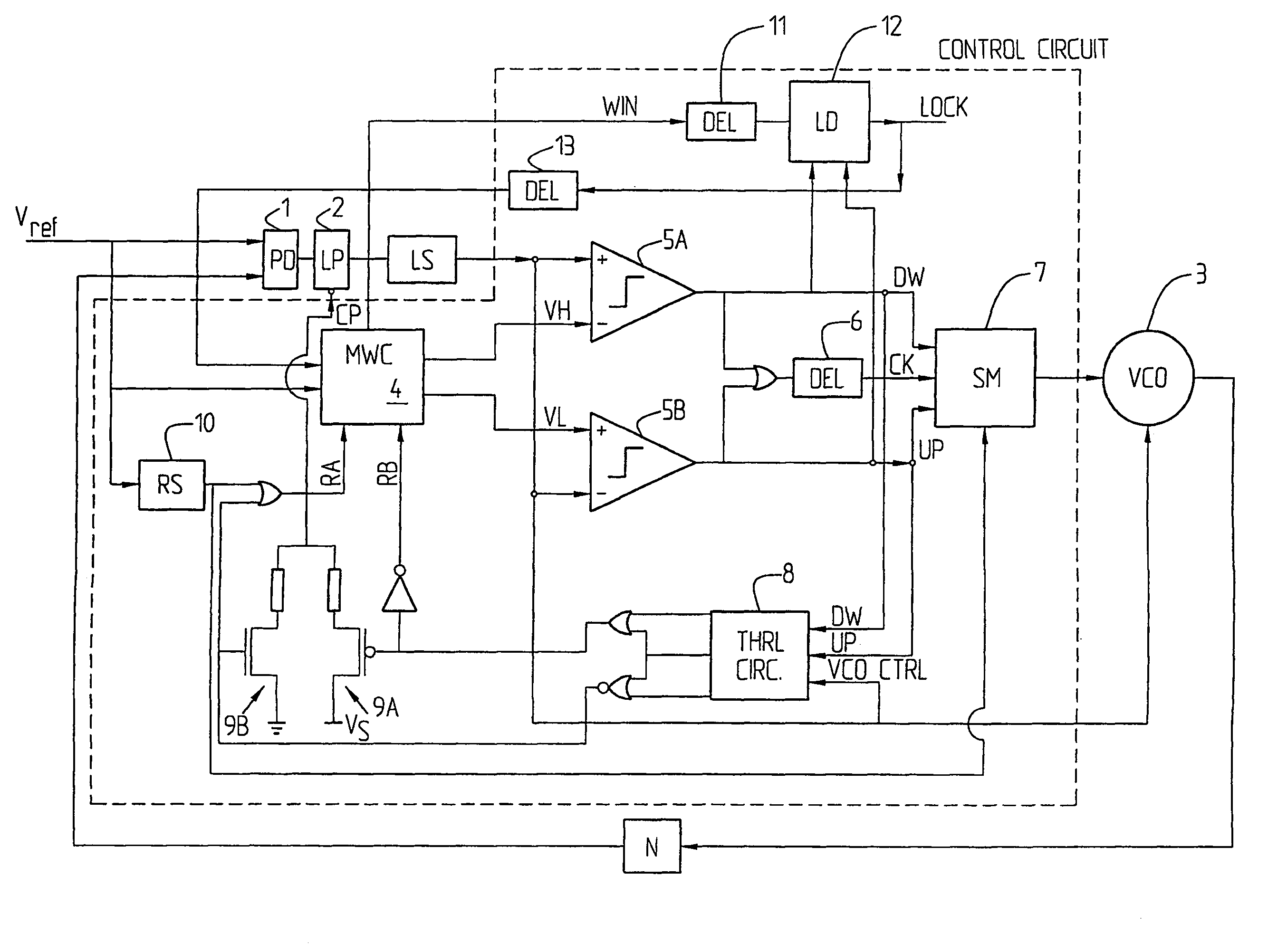
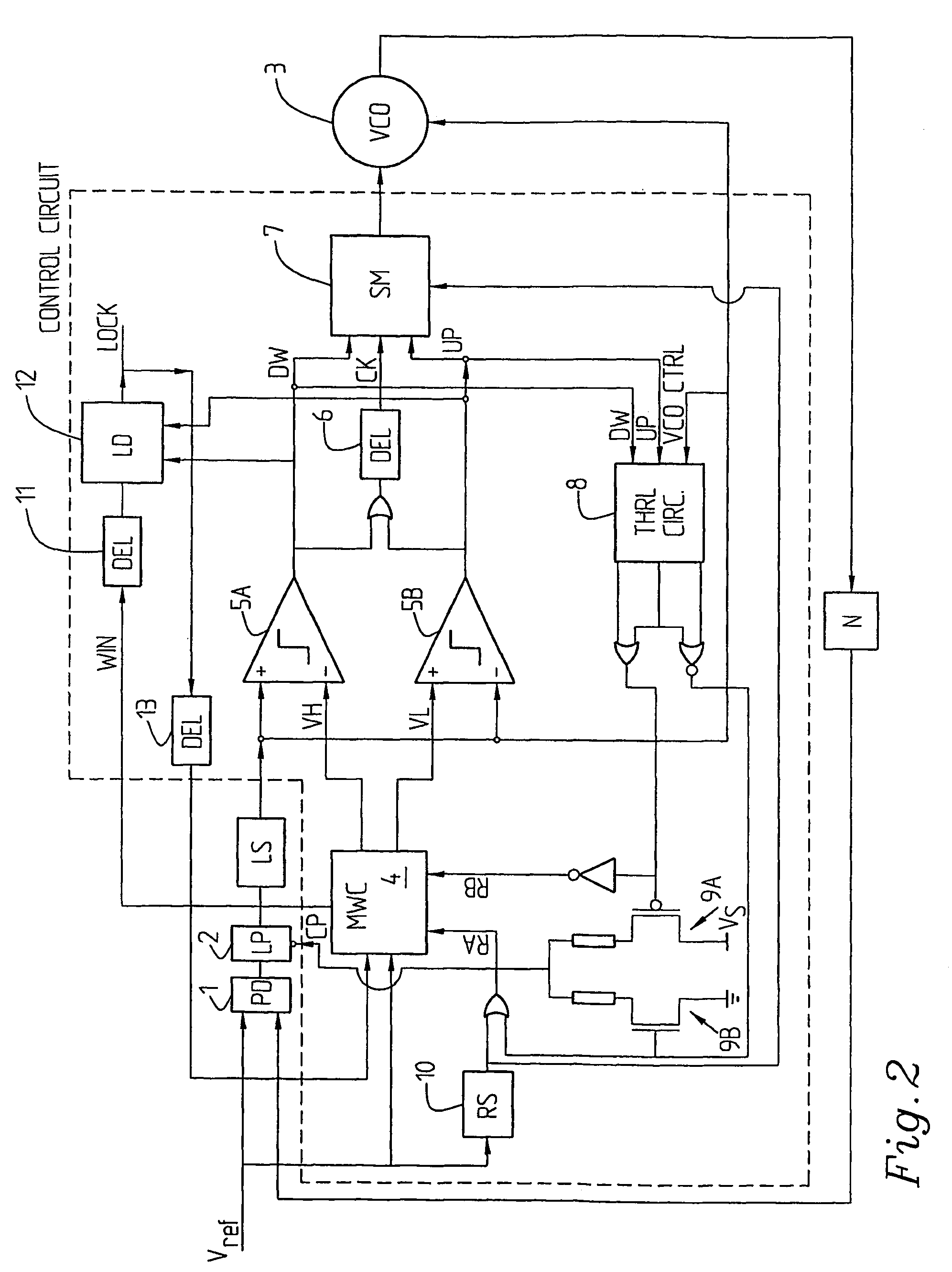
[0051]FIG. 2 shows a PLL arrangement (e.g. for frequency synthesizing) according to an advantageous implementation of the present invention in which a reference voltage Vref is input to a phase detector 1 connected to a loop filter 2. The loop filter 2 advantageously comprises here an active, external or internal, filter as will be more thoroughly described with reference to FIG. 8. In the figure also a level shifter LS is indicated which the signal output from the low pass filter 2 has to pass. This is however not given any reference numeral since it is merely used for adapting an external circuit to the DC level of the control circuit in case it is an external PLL. It is here supposed that the phase detector PD 1, the loop filter LP 2, (a level shifter) and the VCO 3 may be external, the control circuit being indicated through a dashed line. (One or more of the components may also be integrated, i.e. they do not have to be external.)

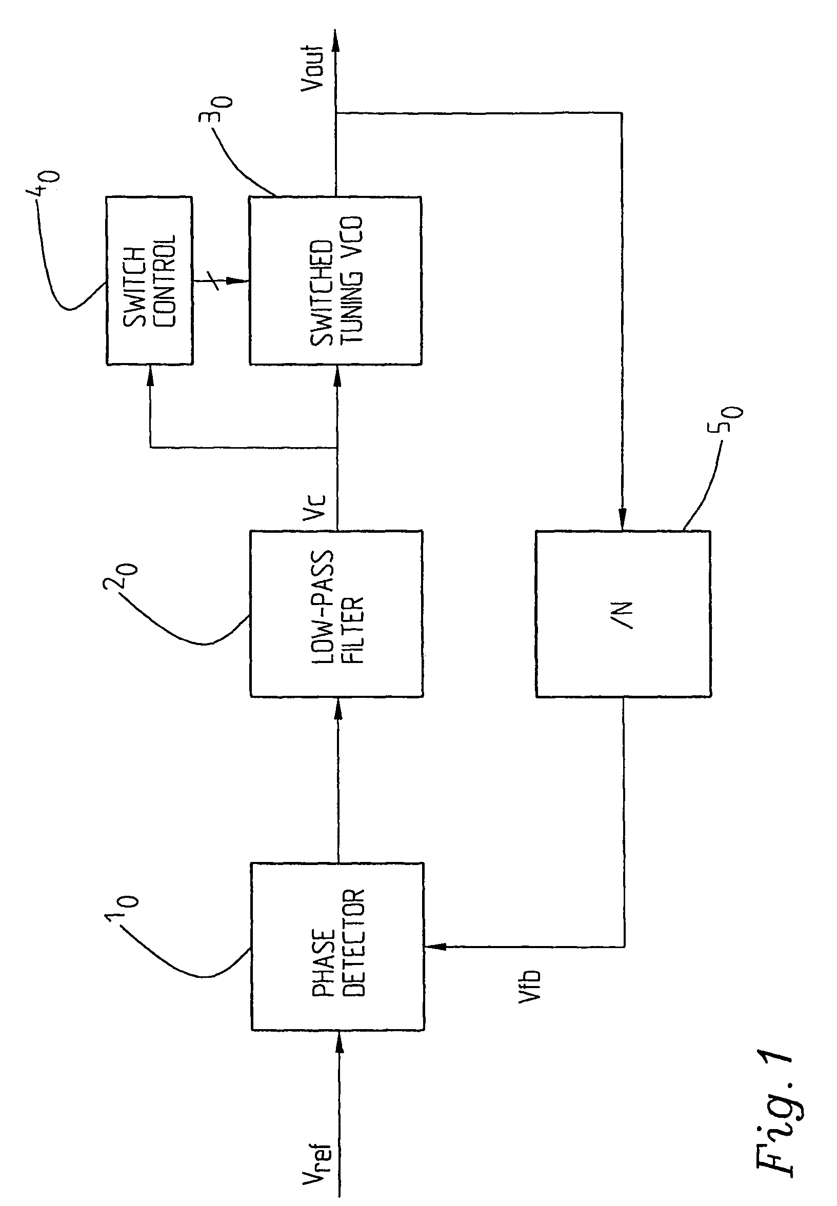
[0052]In an alternative embodiment the arrangeme...


PUM


Abstract

The present invention relates to a multiband PLL arrangement comprising a single loop PLL with a phase / frequency detecting means (1), a loop filter means (2) and a Voltage Controlled Oscillator (VCO) (3), to which PLL a reference voltage signal (Vref) is input. It further comprises a control circuit for appropriately locking the VCO (3) to the correct frequency band, said control circuit comprising a multi-window circuit (4) with at least first and second window amplitudes each defined by respective upper and lower voltage levels, and comparing means (5A, 5B) are provided for comparing a first VCO control voltage output from the loop filter means (2) with the upper and lower voltage levels of a first, broadest amplitude window. If the VCO control voltage settles within said first amplitude window, a narrower window is selected, the voltage levels of which are compared with the VCO control voltage and if the VCO control voltage settles within that or a further subsequent, smaller amplitude window, phase lock is achieved, otherwise, if the VCO control voltage does not settle within said windows, this is established by the comparing means (5A, 5B), said comparing means (5A, 5B) providing a signal for providing a second control signal to the VCO (3) for switching it to another, higher or lower, frequency band. For said other frequency band, the resulting first VCO control voltage signal is compared with said first amplitude window etc. until phase lock is achieved in the appropriate frequency band.

Description

[0001]This application is a U.S. national stage application of International Application No. PCT / SE2003 / 001641 filed Oct. 23, 2003.FIELD OF THE INVENTION[0002]The present invention relates to a multiband PLL (Phase Locked Loop) arrangement comprising a single loop PLL with phase / frequency detecting means, loop filter means and a Voltage Controlled Oscillator. The invention also relates to a method of controlling such a multiband VCO arrangement e.g. such that the VCO locks appropriately in the correct frequency band.STATE OF THE ART[0003]In the society of today wireless communications have developed exceedingly fast and it has been a technical revolution all over the world for communication systems operating at different frequencies for different wireless standards, e.g. from 900 MHz up to 40 GHz, the GHz range being relevant for microwave links. Such microwave links are getting more and more used within mobile telephony systems and for broadband data communication. All these system...

Claims


Application Information

Patent Timeline
Patent Type & Authority Patents(United States)
IPC IPC(8): H03D3/24H03L7/08H03L7/095H03L7/099H03L7/10H03L7/18
CPCH03L7/095H03L7/18H03L7/10H03L7/099H03L7/103
Inventor JACOBSSON, HARALDLOPELLI, EMANUELE
Owner HIGHBRIDGE PRINCIPAL STRATEGIES LLC AS COLLATERAL AGENT
Why Eureka
Try Eureka