Method for manufacturing SOI substrate and SOI substrate

a technology of soi substrate and soi substrate, which is applied in the direction of basic electric elements, electrical apparatus, semiconductor devices, etc., can solve the problems of metal contamination, insufficient function of the gettering layer, and slow diffusion rate of metal impurities in the silicon oxide film rather than in the silicon, so as to achieve efficient manufacturing of the soi substrate and avoid the effect of metal contamination in the device characteristics and excellent gettering ability

Active Publication Date: 2010-07-06
SHIN-ETSU HANDOTAI CO LTD
View PDF21 Cites 3 Cited by
  • Summary
  • Abstract
  • Description
  • Claims
  • Application Information

AI Technical Summary

Benefits of technology

[0010]In view of the above-explained problems, it is an object of the present invention to provide a method for manufacturing an SOI substrate that can efficiently manufacture the SOI substrate having an excellent gettering ability with respect to metal contamination of an SOI layer and to provide the SOI substrate.
[0016]When the time for holding at the temperature in the range of 950° C. to 1100° C. is set to the range of 1 hour to 4 hours in this manner, the sufficient gettering ability can be obtained without reducing productivity.
[0018]As explained above, if the heat treatment atmosphere in at least some of processing steps of the heat treatments is the atmosphere containing water vapor when the heat treatment for holding at the temperature in the range of at least 950° C. to 1100° C. is performed and then the heat treatment at the temperature higher than 1100° C. is carried out as the heat treatment for increasing bonding strength, the gettering ability can be further improved.
[0020]It is known that a concentration of a metal impurity that affects electrical characteristics is 1011 atoms / cm2 level or above. Therefore, when the interface region between the SOI layer and the buried oxide film has the gettering ability of 1×10¹² atoms / cm2 or above like the SOI substrate according to the present invention, degradation in device characteristics due to metal contamination can be sufficiently avoided.
[0021]The method for manufacturing an SOI substrate according to the present invention can efficiently manufacture the SOI substrate having the excellent gettering ability with respect to metal contamination in the SOI layer at a low cost. Furthermore, the SOI substrate according to the present invention can be a high-quality and inexpensive SOI substrate having the sufficiently high gettering ability in an SOI layer.

Problems solved by technology

That is, in many cases, a diffusion rate of a metal impurity is slow in the silicon oxide film rather than in silicon.
Therefore, a harmful effect of the metal contamination becomes more serious as compared with that in a silicon substrate having no SOI structure.
However, even if the same techniques are used to introduce the gettering layer on a support substrate side in the SOI substrate, since a metal impurity hardly passes through the BOX layer, there is a problem that the gettering layer does not sufficiently function, and these techniques cannot be applied to the SOI substrate as they are.
However, such a method has a problem that an increase in the number of processing steps of introducing the impurity results in a rise in cost and a reduction in productivity.
Furthermore, when the impurity introduced for gettering diffuses to reach an active layer of a semiconductor device due to a heat treatment in a manufacturing process of the SOI substrate or in a device process, a harmful effect on electrical characteristics is concerned.
However, this method likewise has a problem that an increase in the number of processing steps of forming the polysilicon layer results in a rise in a cost and a reduction in productivity.
Additionally, when a thickness of the SOI layer is small, forming the polysilicon layer is very difficult.

Method used


Image

  • Method for manufacturing SOI substrate and SOI substrate
  • Method for manufacturing SOI substrate and SOI substrate
  • Method for manufacturing SOI substrate and SOI substrate

Examples


experimental example

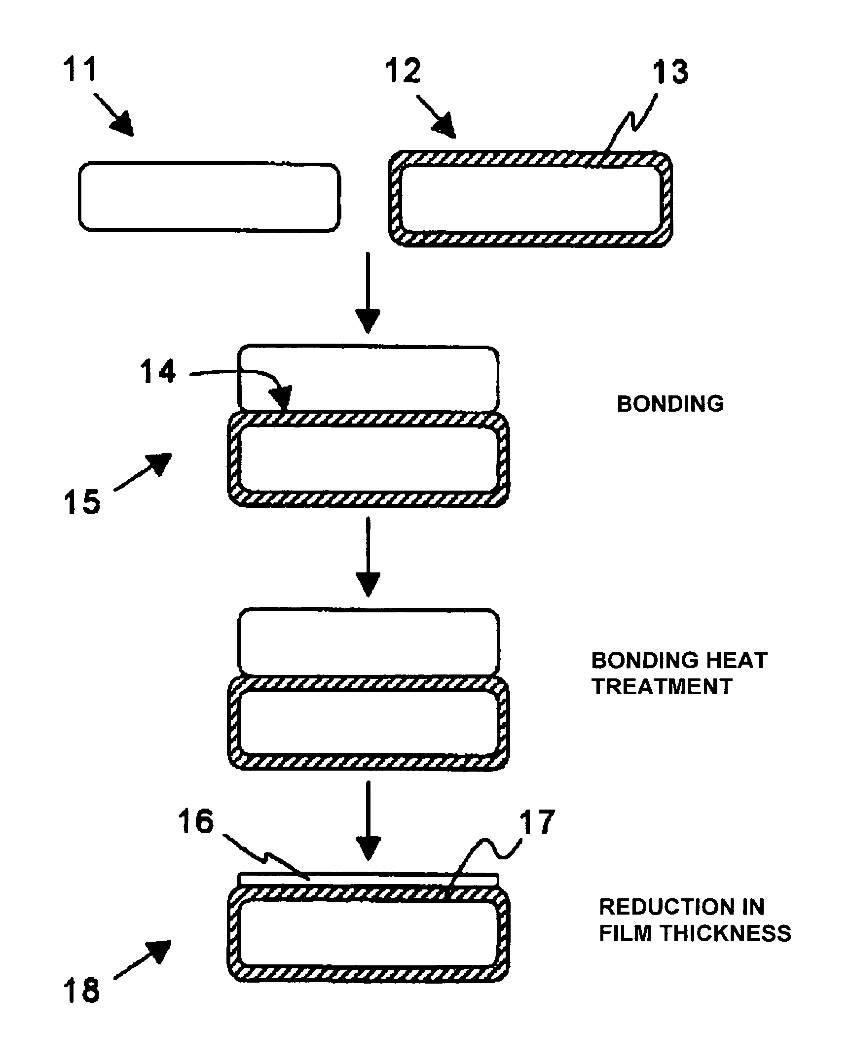
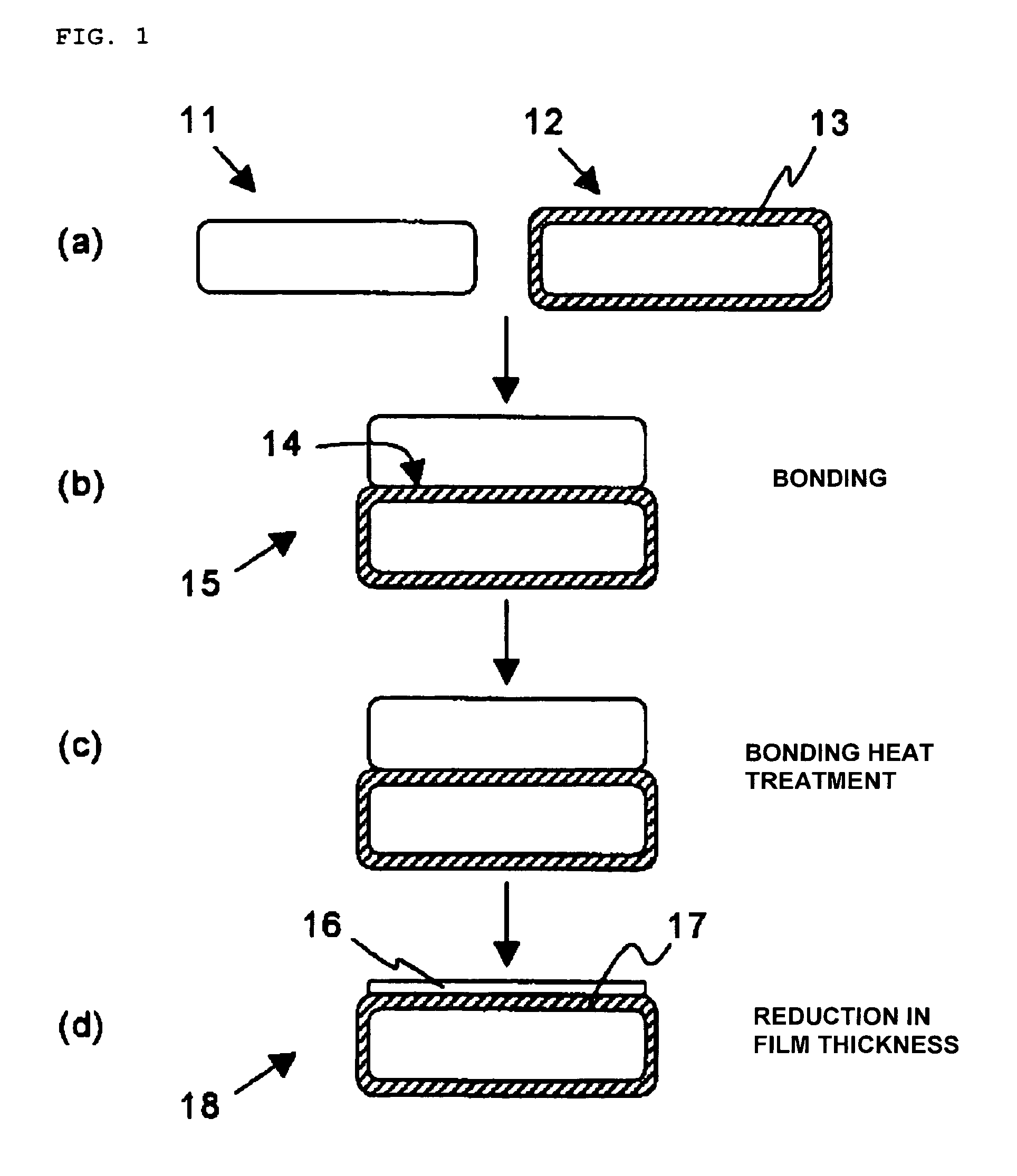
[0036]The present inventors have considered that optimizing a heating temperature at the time of the bonding heat treatment enables improving the gettering ability of a finally manufactured SOI substrate, and conducted the following experiment.

[0037]An experimental example will now be explained with reference to FIG. 1.

[0038]First, two mirror-polished N-type single-crystal silicon substrates each having a diameter of 200 mm and a plane orientation of {100} were prepared. A silicon oxide film 13 serving as a BOX layer and having a film thickness of approximately 1 μm was formed on a surface of a single-crystal silicon substrate 12 functioning as a support substrate based on a thermal oxidation (a). Then, a single-crystal silicon substrate 11 serving as an SOI layer was closely contacted with and bonded to the single-crystal silicon substrate 12 functioning as the support substrate via the silicon oxide film 13 therebetween (b).

[0039]Subsequently, a bonding heat treatment for increasi...

example 1

[0067]An SOI substrate was fabricated based on the processing steps shown in FIG. 1 as follows.

[0068]First, like the experimental example, two mirror-polished N-type single-crystal silicon substrates each having a diameter of 200 mm and a plane orientation of {100} were prepared. A silicon oxide film 13 having a film thickness of approximately 1 μm that becomes a BOX layer was formed on a surface of a single-crystal silicon substrate 12 that becomes a support substrate based on thermal oxidation (a). Then, a single-crystal silicon substrate 11 that becomes an SOI layer was closely contacted with and bonded to the single-crystal silicon substrate 12 that becomes the support substrate via the silicon oxide film 13 therebetween (b).

[0069]Subsequently, a bonding heat treatment for increasing bonding strength was carried out (c). A bonded wafer was put into a heat treatment furnace maintained at 800° C., a temperature was increased to a T2° C. as a holding temperature at a rate of temper...

examples 2 and 3

[0079]Each SOI substrate was fabricated based on the processing steps depicted in FIG. 1 as follows.

[0080]First, like Example 1, two N-type silicon single-crystal substrates were prepared, and a silicon oxide film 13 having a film thickness of approximately 1.3 μm that becomes a BOX layer was formed on a surface of a single-crystal silicon substrate 12 that becomes a support substrate based on thermal oxidation (a). Then, a single-crystal silicon substrate 11 that becomes an SOI layer and the single-crystal silicon substrate 12 that becomes the support substrate were closely contacted with and bonded to each other via the silicon oxide film 13 therebetween (b). Then, a bonded wafer was put into a heat treatment furnace held at 800° C., a temperature was increased to 1000° C. as a holding temperature at a rate of temperature increase of 10° C. / minute, this state was held for 2 hours, then the temperature was increased to 1150° C., this state was maintained for 2 hours, then the tempe...


PUM

PropertyMeasurementUnit
temperatureaaaaaaaaaa

Abstract

According to the present invention, there is provided a method for manufacturing an SOI substrate based on a bonding method, comprising at least: forming a silicon oxide film on a surface of at least one of a single-crystal silicon substrate that becomes an SOI layer and a single-crystal silicon substrate that becomes a support substrate; bonding the single-crystal silicon substrate that becomes the SOI layer to the single-crystal silicon substrate that becomes the support substrate through the silicon oxide film; and performing a heat treatment for holding at a temperature falling within the range of at least 950° C. to 1100° C. and then carrying out a heat treatment at a temperature higher than 1100° C. when effecting a bonding heat treatment for increasing bonding strength. As a result, there are provided the method for manufacturing an SOI substrate that can efficiently manufacture an SOI substrate having an excellent gettering ability with respect to metal contamination in an SOI layer, and the SOI substrate.

Description

TECHNICAL FIELD[0001]The present invention relates to a method for manufacturing an SOI (Silicon On Insulator) substrate based on a bonding method, and more particularly to a method for manufacturing an SOI substrate having an excellent gettering ability with respect to a metal impurity.BACKGROUND ART[0002]As one of semiconductor device substrates, there is an SOI substrate having a silicon layer (which may be referred to as an SOI layer hereinafter) formed on a silicon oxide film as an insulator film. This SOI substrate has characteristics such as a small parasitic capacitance or a high radiation-proof ability since the SOI layer in a substrate surface layer portion serving as a device fabrication region is electrically isolated from the inside of a substrate by a buried oxide film layer (a BOX layer). Therefore, effects such as a high speed / low power consumption operation or prevention of soft-error can be expected, and this substrate has promise as a high-performance semiconducto...

Claims


Application Information

Patent Timeline
Patent Type & Authority Patents(United States)
IPC IPC(8): H01L21/46H01L21/42H01L21/76H01L21/30H01L21/477
CPCH01L21/3226H01L21/76256H01L29/78603H01L21/20
Inventor TAKENO, HIROSHINOTO, NOBUHIKO
Owner SHIN-ETSU HANDOTAI CO LTD
Why Eureka
Try Eureka