Semiconductor device and driving method thereof

a technology of semiconductor devices and driving methods, applied in the direction of digital transmission, pulse techniques, instruments, etc., can solve problems such as circuits not operating normally, and achieve the effects of suppressing the effect of variations in characteristics of semiconductor elements, low cost and high yield

Inactive Publication Date: 2010-07-06
SEMICON ENERGY LAB CO LTD
View PDF34 Cites 1 Cited by
  • Summary
  • Abstract
  • Description
  • Claims
  • Application Information

AI Technical Summary

Benefits of technology

[0006]The invention provides a semiconductor device with high yield by reducing an effect of variations in characteristics of a semiconductor element. Further, the invention provides an inexpensive semiconductor device by improving productivity by reducing the effect of variations in characteristics of a semiconductor element. Furthermore, the invention provides an inexpensive semiconductor device by manufacturing a large amount of semiconductor devices over a large substrate such as a glass substrate or a flexible substrate.
[0022]According to the invention, even in the case where a first demodulation signal generated by the demodulation circuit is incomplete due to an effect of variations in characteristics of a semiconductor element, the first demodulation signal is inputted to a correction circuit to generate a second demodulation signal with equal amplitude to that of a power source voltage. Therefore, by using the invention, an effect of variations in characteristics of a semiconductor element can be suppressed, thereby an inexpensive semiconductor device can be provided by realizing high yield and improving productivity. Further, a semiconductor device of the invention which can be manufactured in a large amount over a large substrate such as a glass substrate or a flexible substrate can be provided at low cost.

Problems solved by technology

In particular, the analog circuit (typically a demodulation circuit) does not operate normally due to the effect of variations in characteristics of semiconductor elements, which is a major factor to reduce yield.

Method used


Image

  • Semiconductor device and driving method thereof
  • Semiconductor device and driving method thereof
  • Semiconductor device and driving method thereof

Examples


embodiment mode 1

[Embodiment Mode 1]

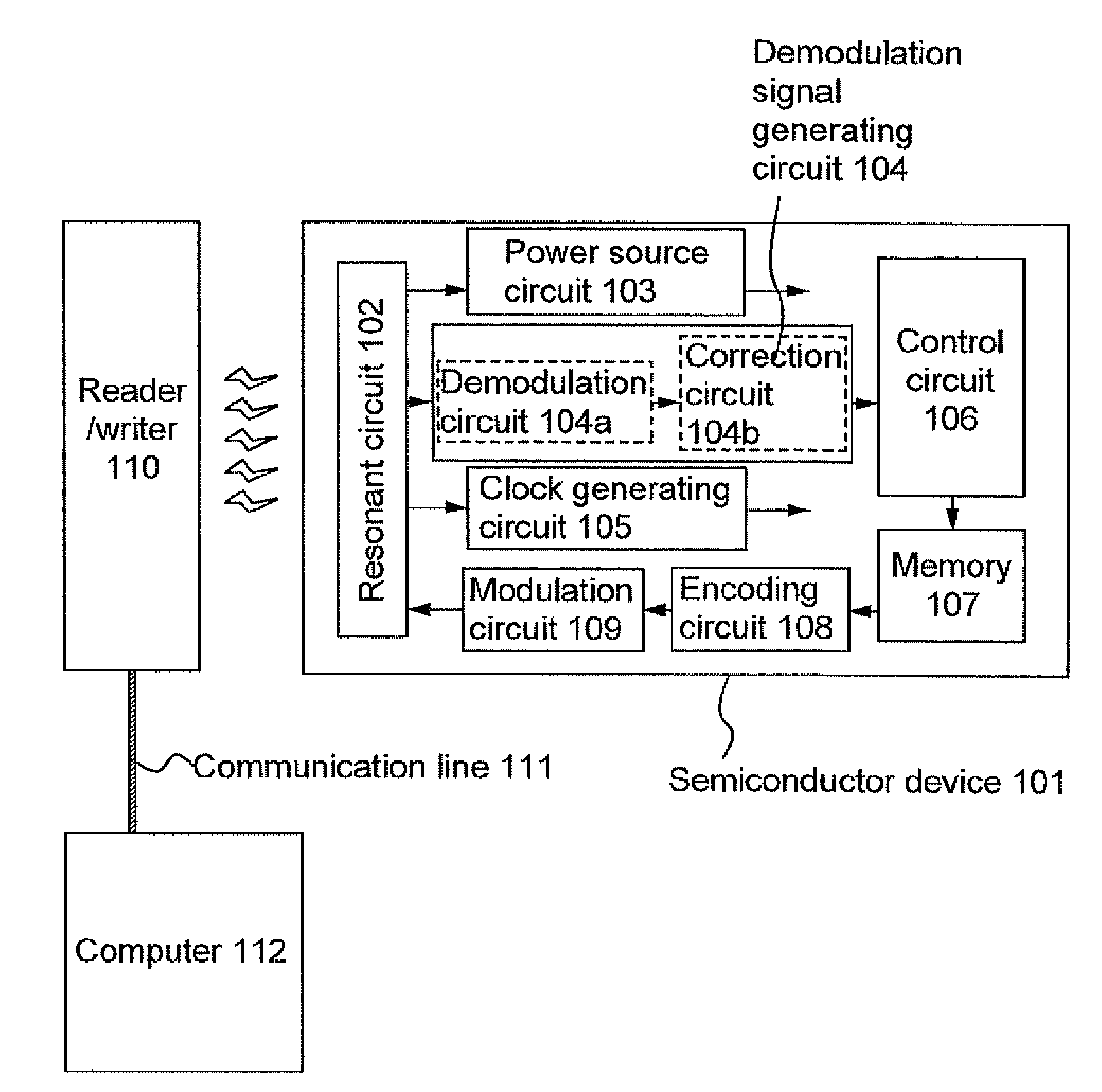
[0032]Description is made with reference to FIG. 1 on a configuration of a semiconductor device of the invention and of a peripheral device thereof. A semiconductor device 101 of the invention transmits and receives data to / from a reader / writer 110 wirelessly through electromagnetic waves. The reader / writer 110 is connected to a computer 112 through a communication line 111. The computer 112 controls communication between the reader / writer 110 and the semiconductor device 101.

[0033]The semiconductor device 101 includes a resonant circuit 102 comprising an antenna and a resonant capacitor, a power source circuit 103, a demodulation signal generating circuit 104, a clock generating circuit 105, a control circuit 106, a memory 107, an encoding circuit 108, and a modulation circuit 109. Further, the semiconductor device 101 does not include an antenna but may include a wire for connecting the antenna in some cases. In these cases, a separately manufactured antenna is ...

embodiment mode 2

[Embodiment Mode 2]

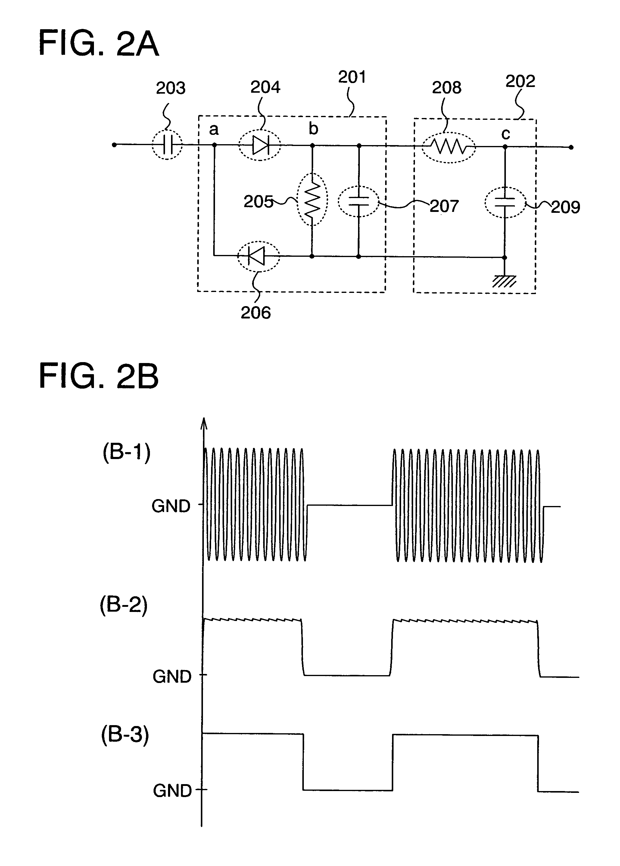
[0055]In this embodiment mode, description is made with reference to FIGS. 5A and 5B on a mode of the correction circuit 104b included in a semiconductor device of the invention, which is different from Embodiment Mode 1. The circuits shown in FIGS. 5A and 5B are differential amplifiers.

[0056]FIGS. 5A and 5B show differential amplifiers each of which has a configuration to compare a voltage generated at the middle of VDD and GND using resistance division and the first demodulation signal outputted from the demodulation circuit 104a. By controlling the level of the voltage generated by the resistance division, the variations in the first demodulation signal shown in the example of FIGS. 3A to 3D can be corrected. FIG. 5A is suitable for correcting the cases (FIGS. 3A and 3B) where the Hi level of the first demodulation signal becomes lower than VDD. On the contrary, FIG. 5B is suitable for correcting the case (FIG. 3C) where the Lo level of the first demodulation s...

embodiment 1

[0061]A semiconductor device of the invention is mainly formed of semiconductor elements. In this embodiment, description is made with reference to cross sectional diagrams on an example of manufacturing the semiconductor elements. Hereafter, the semiconductor elements are collectively referred to as an element group.

[0062]In this embodiment, an element group is formed over a glass substrate. After that, the element group is peeled off the substrate and attached to a flexible substrate (including a film and the like) in order to provide added values such as lightweight and flexibility to the semiconductor device.

[0063]First, a peeling layer 4002 is formed over a glass substrate 4001 (see FIG. 6A). The substrate may be formed of quartz, silicon, metal, and the like as well as glass. The peeling layer 4002 is formed over an entire surface or a part of the substrate using an element such as a metal or silicon, or a compound thereof, or the like. It is to be noted that the peeling layer...


PUM


Abstract

The invention provides a semiconductor device with high yield by reducing an effect of variations in characteristics of a semiconductor element. Further, by reducing an effect of variations in characteristics of a semiconductor element to improve productivity, an inexpensive semiconductor device can be provided. Further, an inexpensive semiconductor device can be provided by forming a semiconductor device in a large amount over a large substrate such as a glass substrate and a flexible substrate. A semiconductor device of the invention includes a demodulation signal generating circuit and an antenna or a wire for connecting the antenna. The demodulation signal generating circuit includes a demodulation circuit and a correction circuit. The correction circuit corrects a first demodulation signal generated from the demodulation circuit and generates a second demodulation signal.

Description

BACKGROUND OF THE INVENTION[0001]1. Field of the Invention[0002]The present invention relates to a semiconductor device capable of transmitting / receiving data wirelessly and a driving method thereof.[0003]2. Description of the Related Art[0004]In recent years, a semiconductor device capable of transmitting / receiving data wirelessly has been advanced and attracting attentions. Such a semiconductor device is, for example, an RFID (Radio Frequency Identification), an RF chip, an RF tag, an IC chip, an IC tag, a wireless chip, a wireless tag, an electron chip, an electron tag, a wireless processor, or a wireless memory, which is already introduced into some markets. Among them, a semiconductor device for managing objects is advanced, which is small, lightweight, easy to use, high in security, and low cost.SUMMARY OF THE INVENTION[0005]A semiconductor device which can transmit / receive data wirelessly is formed of an analog circuit which receives and transmits data through electromagnetic...

Claims


Application Information

Patent Timeline
Patent Type & Authority Patents(United States)
IPC IPC(8): H03K9/00G06K19/06
CPCG06K19/07749H01L27/13H01L27/1266H01L27/1214
Inventor KATO, KIYOSHISHIONOIRI, YUTAKA
Owner SEMICON ENERGY LAB CO LTD
Why Eureka
Try Eureka