Nonvolatile semiconductor memory device and method of manufacturing the same

a semiconductor memory and non-volatile technology, applied in the direction of semiconductor devices, electrical devices, transistors, etc., can solve the problems of large capacitance decrease the inability of related-art ono films to be used as inter-electrode insulating films, and the inherent problems of materials, so as to prevent the deterioration of the inter-electrode insulating film, reduce the effective capacitance, and good cell operation characteristics

Active Publication Date: 2010-07-13
KIOXIA CORP
View PDF8 Cites 6 Cited by
  • Summary
  • Abstract
  • Description
  • Claims
  • Application Information

AI Technical Summary

Benefits of technology

[0028]The present invention has been made in view of the above circumstances and provides a nonvolatile semiconductor memory device and method of manufacturing the same. According to an aspect of the present invention, a nonvolatile semiconductor memory device has good cell operation characteristics and can prevent deterioration of an inter-electrode insulating film of the memory cell without decreasing effective capacitance.

Problems solved by technology

The related-art ONO film can not be used as the inter-electrode insulating film in the plainer cell structure since the leakage current suddenly increases in the high electric field.
However, these materials have their inherent problem in the conventional manufacturing method as described below.
Accordingly, the dielectric constant of the inter-electrode insulating film formed on the floating gate electrode made of a Si containing conductive material such as polycrystalline silicon decreases with increasing the physical thickness due to large Si diffusion by the above-mentioned rapid thermal treatment, which is required in a device manufacturing process, resulting in large capacitance decrease of the inter-electrode insulating film.
Such deterioration of the inter-electrode insulating film raises a problem of insufficient performance in writing, eraseing, reading, and data retaining of the memory cell.
In addition, as the dielectric constant decreases, breakdown voltage decreases to 20 MV / cm or so while the leakage current density increases up to 1×10⁻² A / cm2, which do not satisfy the device specification.
Since SiN or Al2O3 has a dielectric constant lower than that of metal oxynitride including rare-earth elements, effective capacitance of the inter-electrode insulating film is reduced, resulting in deteriorating performance of the memory cell.
As described above, there is a serious problem that Si in the silicon substrates or polycrystalline silicon adjacent to the inter-electrode insulating film diffuses in large quantities into the inter-electrode insulating film, which is made of rare-earth oxide, rare-earth nitride or rare-earth oxynitride, by thermal treatment.
In particulary, the problem is the large quantities of Si diffusion and its uncontrollability.
As rare-earth oxide, rare-earth nitride or rare-earth oxynitride including rare-earth elements with high dielectric constants is used as the inter-electrode insulating film in the memory cell with the floating gate electrode, quality of the inter-electrode insulating film is deteriorated due to the thermal treatment after deposition of the inter-electrode insulating film.
Therefore, the dielectric constant is decreased, resulting in deterioration in leakage current characteristics.
Accordingly, such a memory device can not achieve high-performances in writing, erasing, reading, and data retaining of the memory cell.

Method used


Image

  • Nonvolatile semiconductor memory device and method of manufacturing the same
  • Nonvolatile semiconductor memory device and method of manufacturing the same
  • Nonvolatile semiconductor memory device and method of manufacturing the same

Examples


first embodiment

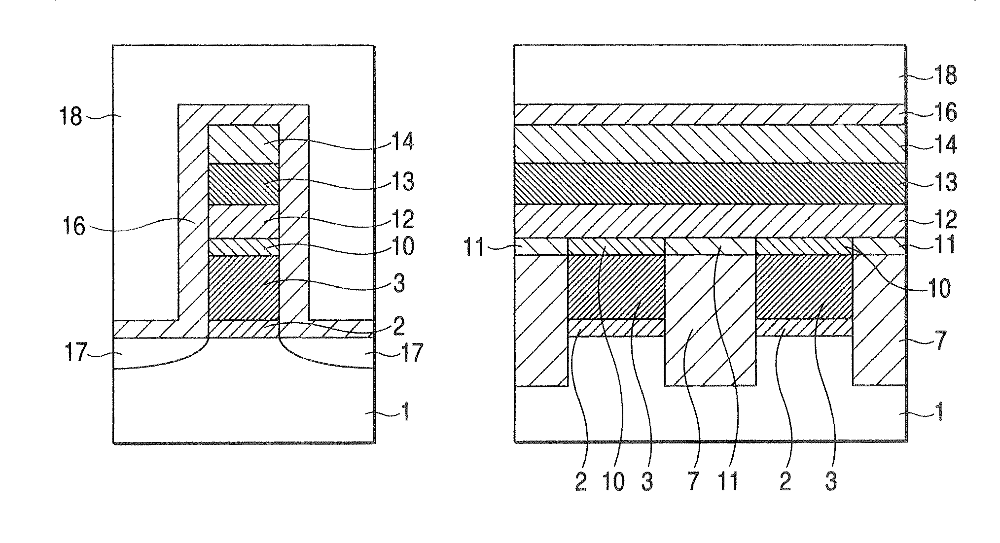
[0046]Hereinafter, a structure of a memory cell of an NAND nonvolatile semiconductor memory device according to a first embodiment of the invention will be described with reference to FIG. 1.

[0047]An NAND nonvolatile semiconductor memory device comprises bit lines, select gate transistors that interconnect memory cells through the bit lines, the memory-cells connected in series by the bit lines that are placed under the bit liens. FIG. 1 shows cross-sectional structures of a memory cell. The left figure of FIG. 1 is a cross-sectional view in a word line direction. The right figure of FIG. 1 is a cross-sectional view in a direction perpendicular to the word line direction. The right and left figures of FIG. 1 are perpendicular to each other.

[0048]As shown in FIG. 1, source-and drain regions 17 doped with predetermined impurities are formed on a silicon substrate 1. An about 6˜7 nm thick silicon oxide film 2 as a tunneling insulating film is formed between the source-and drain regions...

second embodiment

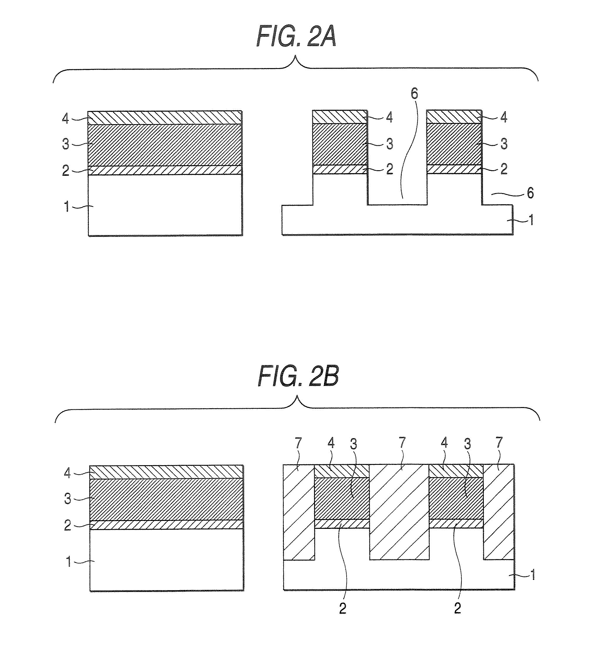
[0094]Hereinafter, a structure of a memory cell of an NAND nonvolatile semiconductor memory device and a method of manufacturing the same according to a second embodiment of the invention will be described with reference to FIG. 5.

[0095]FIG. 5 is a cross-sectional view in a direction perpendicular to a word line of a memory cell.

[0096]As shown in FIG. 5, source and drain regions (not shown) are formed on a silicon substrate 21 doped with predetermined impurities therein. An about 6˜7 nm thick silicon oxide film 22 as a tunneling insulating film is formed between the source and drain regions on the silicon substrate 21. On the silicon oxide film 22 are stacked a 40 nm thick polycrystalline silicon layer 23 as a floating gate electrode, which is made of a Si containing conductive material, a WSi2 layer 24 as a metal silicide layer, a LaHfON layer 25 and a HfAlOx layer 26 as an inter-electrode insulating film, and a conductive layer 27 as a control gate electrode having a double-layere...


PUM

PropertyMeasurementUnit
temperatureaaaaaaaaaa
depthaaaaaaaaaa

Abstract

A memory cell in a nonvolatile semiconductor memory device includes a tunneling insulating film, a floating gate electrode made of a Si containing conductive material, an inter-electrode insulating film made of rare-earth oxide, rare-earth nitride or rare-earth oxynitride, a control gate electrode, and a metal silicide film formed between the floating gate electrode and the inter-electrode insulating film.

Description

CROSS-REFERENCE TO RELATED APPLICATIONS[0001]This application is based on and claims the benefit of priority from the prior Japanese Patent Application No. 2006-067640, filed on Mar. 13, 2006; the entire contents of which are incorporated herein by reference.BACKGROUND[0002]1. Technical Field[0003]The present invention relates to a nonvolatile semiconductor memory device which is capable of improving performance of memory cells and reducing leakage current by using high dielectric materials for an inter-electrode insulating film in a stack gate structure having a floating gate electrode, and a method of manufacturing the same.[0004]2. Description of Related Art[0005]An NAND flash memory (one of nonvolatile semiconductor memory devices) will be hereinafter described by way of an example.[0006]A memory cell of an NAND volatile semiconductor memory device has a stack structure in which a tunneling insulating film and a floating gate electrode are formed on a semiconductor substrate and...

Claims


Application Information

Patent Timeline
Patent Type & Authority Patents(United States)
IPC IPC(8): H01L29/788
CPCH01L21/28273H01L27/115H01L27/11521H01L29/42324H01L29/513H01L29/7885H01L29/40114H10B69/00H10B41/30H01L21/28052
Inventor NISHIKAWA, YUKIETAKASHIMA, AKIRASHIMIZU, TATSUO
Owner KIOXIA CORP
Why Eureka
Try Eureka