Semiconductor integrated circuit

a technology of integrated circuits and semiconductors, applied in semiconductor lasers, instruments, relays, etc., can solve problems such as inability to perfectly reduce voltage variation to zero, circuit operation becomes unstable, and reduce the reliability of memory, so as to improve the reliability and operation speed of semiconductor integrated circuits, and achieve excellent reliability. , the effect of high speed operation

Active Publication Date: 2010-07-27
NEC CORP
View PDF12 Cites 0 Cited by
  • Summary
  • Abstract
  • Description
  • Claims
  • Application Information

AI Technical Summary

Benefits of technology

[0028]An object of the present invention is to provide a semiconductor integrated circuit that can prevent an internal voltage from the voltage generating circuit from varying during a long term.
[0029]Another object of the present invention is to provide a technique that can improve the reliability and operation speed of a semiconductor integrated circuit.
[0030]Still another object of the present invention is to-provide an MRAM that has an excellent reliability and can attain a high speed operation.
[0032]Thus, it is possible to prevent the current from flowing between the voltage generating circuit and the first capacitance for the period during which the function circuit is activated. As a result, the above-mentioned accumulation phenomenon of the voltage variation is prevented. Thus, the long-term variation in the reference voltage that is supplied to the function circuit from the voltage generating circuit is prevented, thereby improving the reliability in the semiconductor integrated circuit. Also, the operation of the function circuit is not required to be kept waiting until the reference voltage is stabilized. Therefore, the operation speed of the semiconductor integrated circuit is improved. In this way, according to the present invention, the semiconductor integrated circuit that has the excellent reliability, yield and operation speed is provided.
[0038]According to the semiconductor integrated circuit according to the present invention, it is possible to prevent the internal voltage from the voltage generating circuit from varying for the long-term. Thus, the reliability and operation speed of the semiconductor integrated circuit are improved. In particular, the MRAM that has the excellent reliability and can attain the high speed operation can be provided.

Problems solved by technology

However, because of the circuit operation, it is impossible to perfectly reduce the voltage variation to zero.
Thus, even in case of the very small voltage variation such as about several μV, when the voltage variation is accumulated, there is a possibility that the circuit operation becomes unstable.
Therefore, the accumulated voltage variation causes erroneous write and reduces the reliability of a memory.
However, as shown in FIG. 5, when a next write operation starts at a time t3 before the gate voltage Vp2 is perfectly returned to the voltage level Vp1, a problem is caused.
The repetition of such an operation results in the accumulation of the differences between the gate voltage Vp2 and the voltage level Vp1.
Thus, it becomes impossible to insure the stable write operation.
As shown in FIG. 4, even in case of the voltage variation of several mV, there is a risk that the write current variation of several % is caused.
This leads to an erroneous operation at the time of write and results in reduction in the reliability of the MRAM.
As mentioned above, the related-art semiconductor integrated circuit has the difficulty that the influence of the coupling of the parasitic capacitance causes the internal voltage from the voltage generating circuit 101 to be greatly varied in the long term.
This leads to the erroneous operation of the function circuit 102 that operates in accordance with the internal voltage.

Method used


Image

  • Semiconductor integrated circuit
  • Semiconductor integrated circuit
  • Semiconductor integrated circuit

Examples


first exemplary embodiment

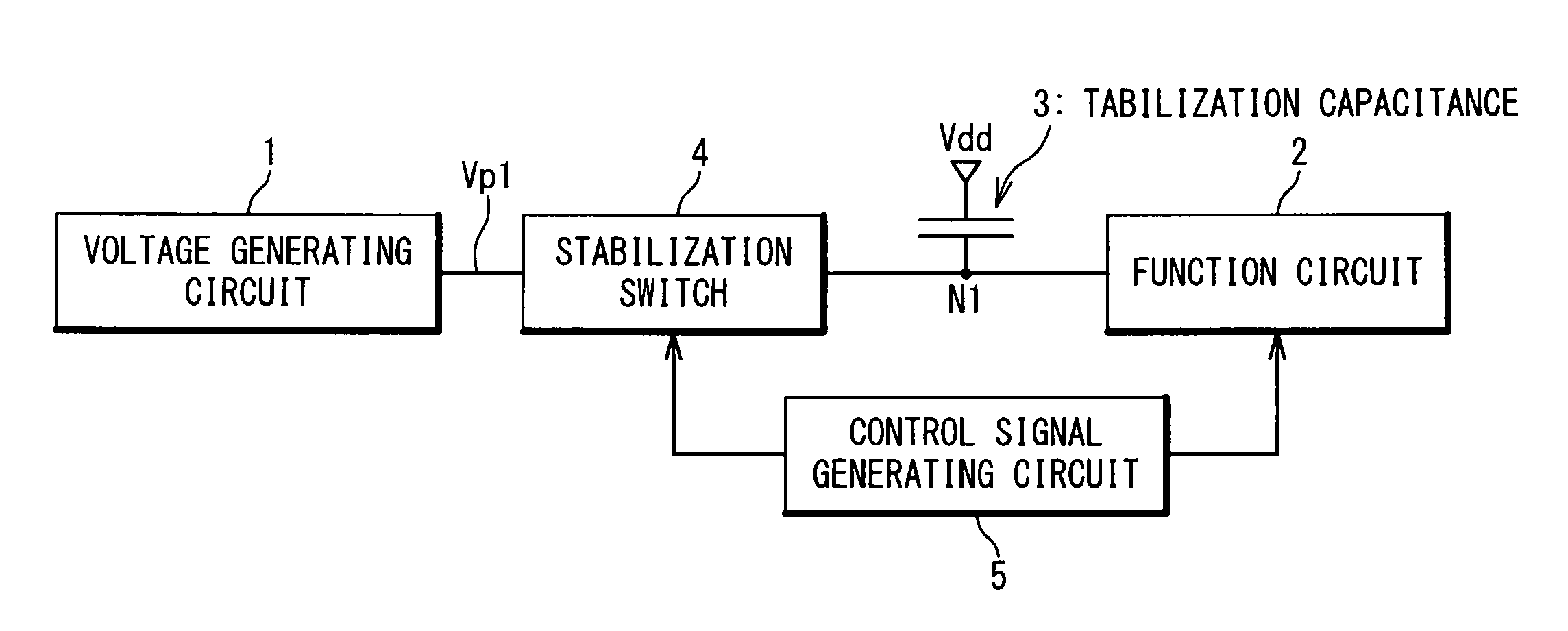
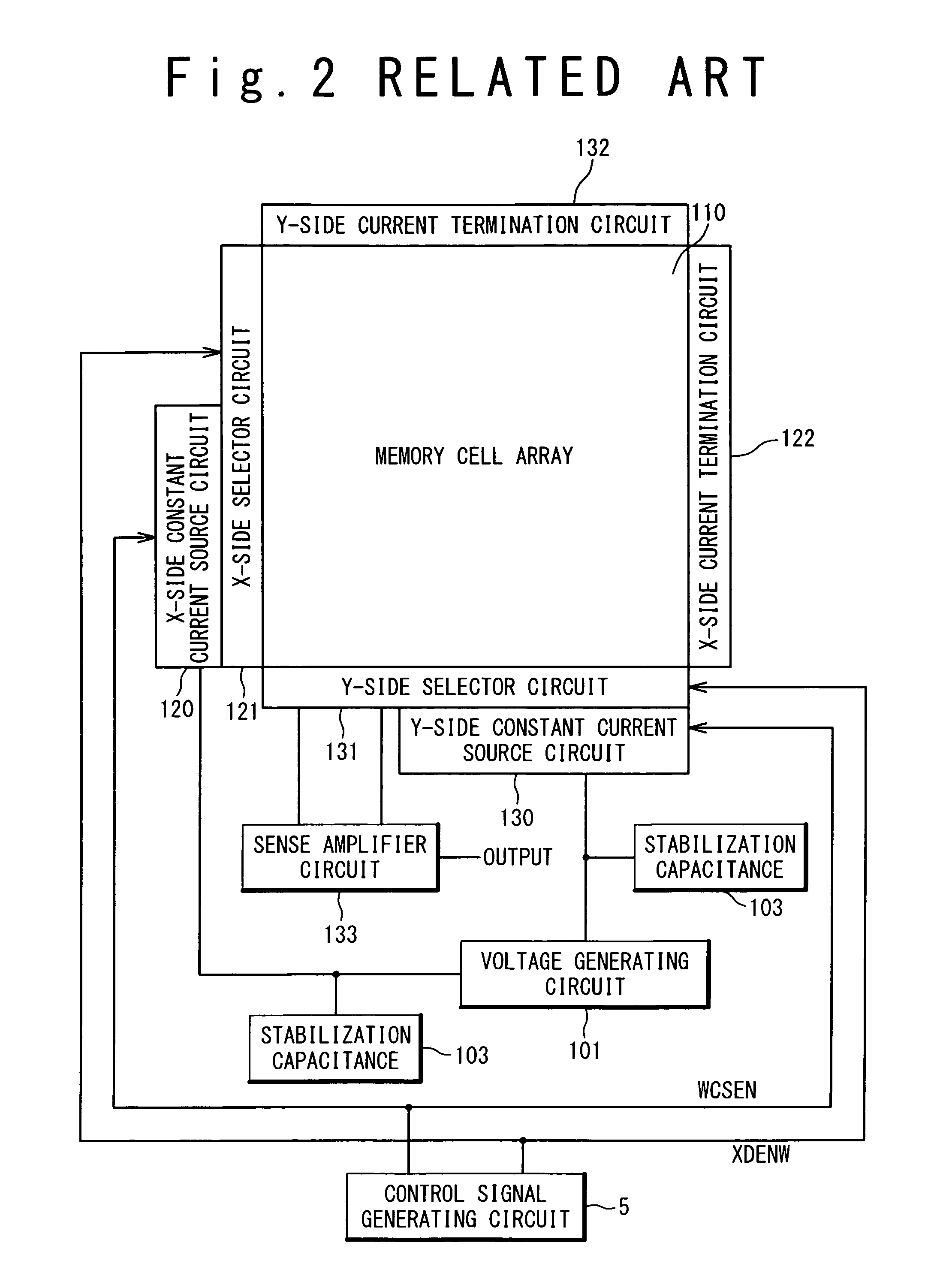
[0072]FIG. 9 is a block diagram showing the configuration of the MRAM according to the first exemplary embodiment of the present invention. This MRAM contains a memory cell array 10, an X-side constant current source circuit 20, an X-side selector 21, an X-side current termination circuit 22, a Y-side constant current source circuit 30, a Y-side selector 31, a Y-side current termination circuit 32 and a sense amplifier circuit 33. Moreover, the MRAM contains the voltage generating circuit 1, the stabilization capacitances 3, the stabilization switches (SSW) 4 and the control signal generating circuit 5 that are shown in FIG. 8. In this case, the X-side constant current source circuit 20 or the Y-side constant current source circuit 30 corresponds to the function circuit 2, and this operates in accordance with the voltage generated by the voltage generating circuit 1. The stabilization capacitance 3 is inserted in parallel between the voltage generating circuit 1 and the current sour...

second exemplary embodiment

[0093]The semiconductor integrated circuit according to the second exemplary embodiment will be described below. According to this exemplary embodiment, the voltage variation in the output voltage Vp1 that is caused by the coupling noise current Ip (refer to FIG. 12) in the first exemplary embodiment is reduced. Thus, when the output voltage Vp1 of the voltage generating circuit 1 is used in another function circuit, this exemplary embodiment is especially preferable.

[0094]FIG. 14 is a block diagram showing the configuration of the MRAM according to the second exemplary embodiment and corresponds to FIG. 9 in the first exemplary embodiment. In FIG. 14, the same reference numerals and symbols are assigned to the same components as those of FIG. 9, and the explanations are properly omitted. Similarly to the first exemplary embodiment, the stabilization capacitances 3 are inserted in parallel between the current source circuits (the function circuits) 20 and 30 and the stabilization sw...

third exemplary embodiment

[0104]The semiconductor integrated circuit according to the third exemplary embodiment of the present invention will be described below. According to this exemplary embodiment, the stabilization switch 4 is applied to an analog circuit that requires a plurality of stabilization capacitances 3.

[0105]FIG. 17 is a block diagram showing the configuration of the MRAM according to the third exemplary embodiment and corresponds to FIG. 9 in the first exemplary embodiment. In FIG. 17, the same reference numerals and symbols are assigned to the same components as those of FIG. 9, and the explanations thereof are properly omitted. In this exemplary embodiment, each of the current source circuits (function circuits) 20 and 30 is connected through a plurality of routes to the voltage generating circuit 1. The voltage generating circuit 1 generates a plurality of kinds of voltages (Vp1, Vp3) as the reference voltages for the plurality of routes. Each of the current source circuits 20 and 30 rece...


PUM


Abstract

A semiconductor integrated circuit is provided that can prevent an internal voltage from the voltage generating circuit from varying during a long term. The semiconductor integrated circuit of the present invention includes a voltage generating circuit configured to generate a reference voltage; a function circuit configured to operate by using the reference voltage; a first capacitance connected to a first node between the voltage generating circuit and the function circuit; and a switch provided between the voltage generating circuit and the first node. The switch is in a turned-off state at least for a period during which the function circuit is in an activated state.

Description

TECHNICAL FIELD[0001]The present invention relates to a semiconductor integrated circuit. More particularly, the present invention relates to a semiconductor integrated circuit that contains a voltage generating circuit for generating an internal voltage.BACKGROUND ART[0002]Generally, in a semiconductor integrated circuit, desirable voltages other than power supply voltages are internally generated by a voltage generating circuit. The generated internal voltages are used in analog circuits such as a current source, a sense amplifier, and a different voltage generating circuit. In order to minimize a variation of the voltage generated by the voltage generating circuit, the output of the voltage generating circuit is typically connected to one end of a stabilization capacitance.[0003]Such a configuration is described in Japanese Patent Application Publications (JP-P2002-111470A, JP-P2003-22697A, JP-P2005-6489A, JP-P2004-220759A, JP-P2002-208275A, and JP-P2004-259318A).[0004]In the Jap...

Claims


Application Information

Patent Timeline
Patent Type & Authority Patents(United States)
IPC IPC(8): G11C5/14H01S3/00H01S3/10H01S3/13H01S3/131H01S5/0683H01S5/0687
CPCG11C5/147H01S3/005H01S3/10076G11C11/1675G11C11/1693G11C11/1697
Inventor HONDA, TAKESHISAKIMURA, NOBORUSUGIBAYASHI, TADAHIKO
Owner NEC CORP
Why Eureka
Try Eureka