Copper pillar tin bump on semiconductor chip and method of forming the same

a technology of copper pillars and semiconductor chips, which is applied in the direction of semiconductor devices, semiconductor/solid-state device details, electrical apparatus, etc., can solve the problems of limiting the minimum pattern size, the minimum pitch of metal masks and solder paste printing resolution, and the minimum pattern size restriction, so as to reduce the pitch of copper pillar tin bumps and high density packaging. , the effect of high density

Inactive Publication Date: 2010-08-24
HWABEAK ENG
View PDF11 Cites 31 Cited by
  • Summary
  • Abstract
  • Description
  • Claims
  • Application Information

AI Technical Summary

Benefits of technology

[0010]The purpose of the present invention is to solve above-described problems, and is to provide copper pillar tin bump on semiconductor chip and method of forming of the same which has a minute pattern composed by exposure that makes it possible to form a high density packaging by reducing a pitch of copper pillar tin bump.
[0011]Another purpose of the present invention is to provide copper pillar tin bump on semiconductor chip and method of forming of the same which is possible to form the high density packaging by simple progress of single photoresist patterning progress.
[0012]Another purpose of the present invention is to provide copper pillar tin bump on semiconductor chip and method of forming of the same which signal delay can be reduced by reduced parasite resistance because of low electric resistance.

Problems solved by technology

Such packaging techniques was solder paste screen painting by using screen printer, but it has limitation of minimum pattern size, restriction of minimum pitch of metal mask and solder paste printing resolution to make high density semiconductor chip packaging.
On the other hand, high density chip packaging techniques has been developed by using tin electroplating recently, but in this way, parasite resistance can be occurred by small packaging thickness between chip and board and thin insulation layer among boards, and it can have problem with durability because it is not good enough to be a mechanical stress absorption layer.

Method used


Image

  • Copper pillar tin bump on semiconductor chip and method of forming the same
  • Copper pillar tin bump on semiconductor chip and method of forming the same
  • Copper pillar tin bump on semiconductor chip and method of forming the same

Examples


Embodiment Construction

[0035]Hereinafter, the present utility is described in detail with reference to the attached drawings.

[0036]Before the detailed description, it should be noted that the terms used in the present specification and the claims are not to be limited to their lexical meanings, but are to be interpreted to conform with the technical idea of the present invention under the principle that the inventor can properly define the terms for the best description of the invention made by the inventor.

[0037]Therefore, the embodiments and the constitution illustrated in the attached drawings are merely preferable embodiments according to the present invention, and thus they do not express all of the technical idea of the present invention, so that it should be understood that various equivalents and modifications can exist which can replace the embodiments described in the time of the application.

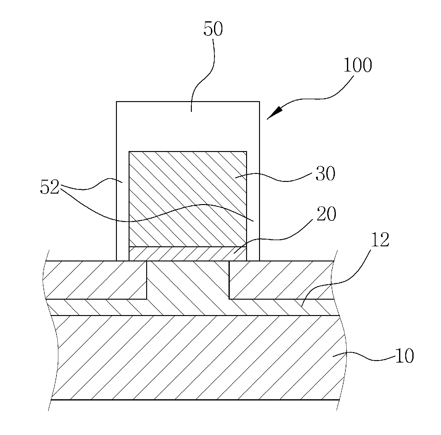
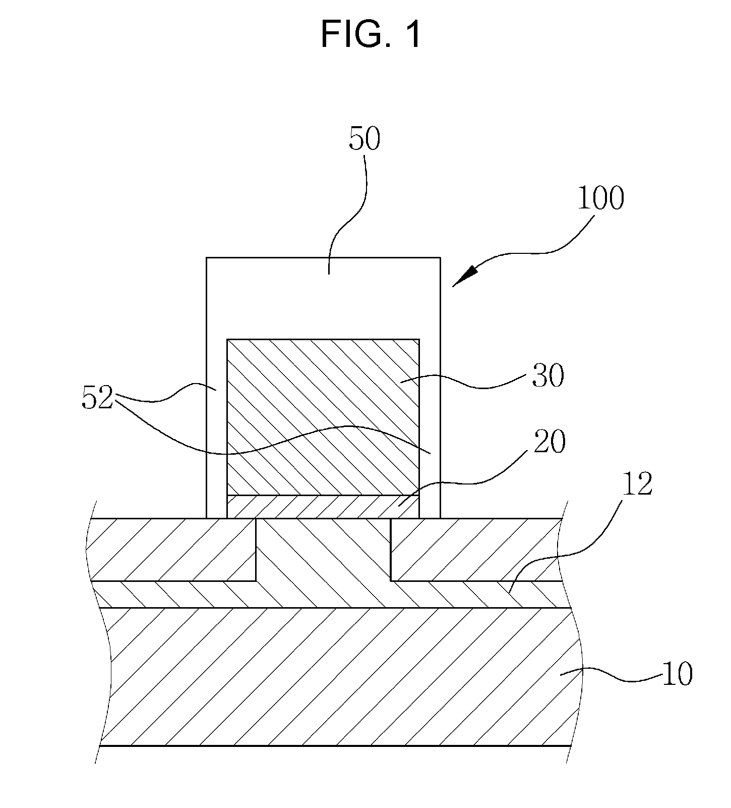
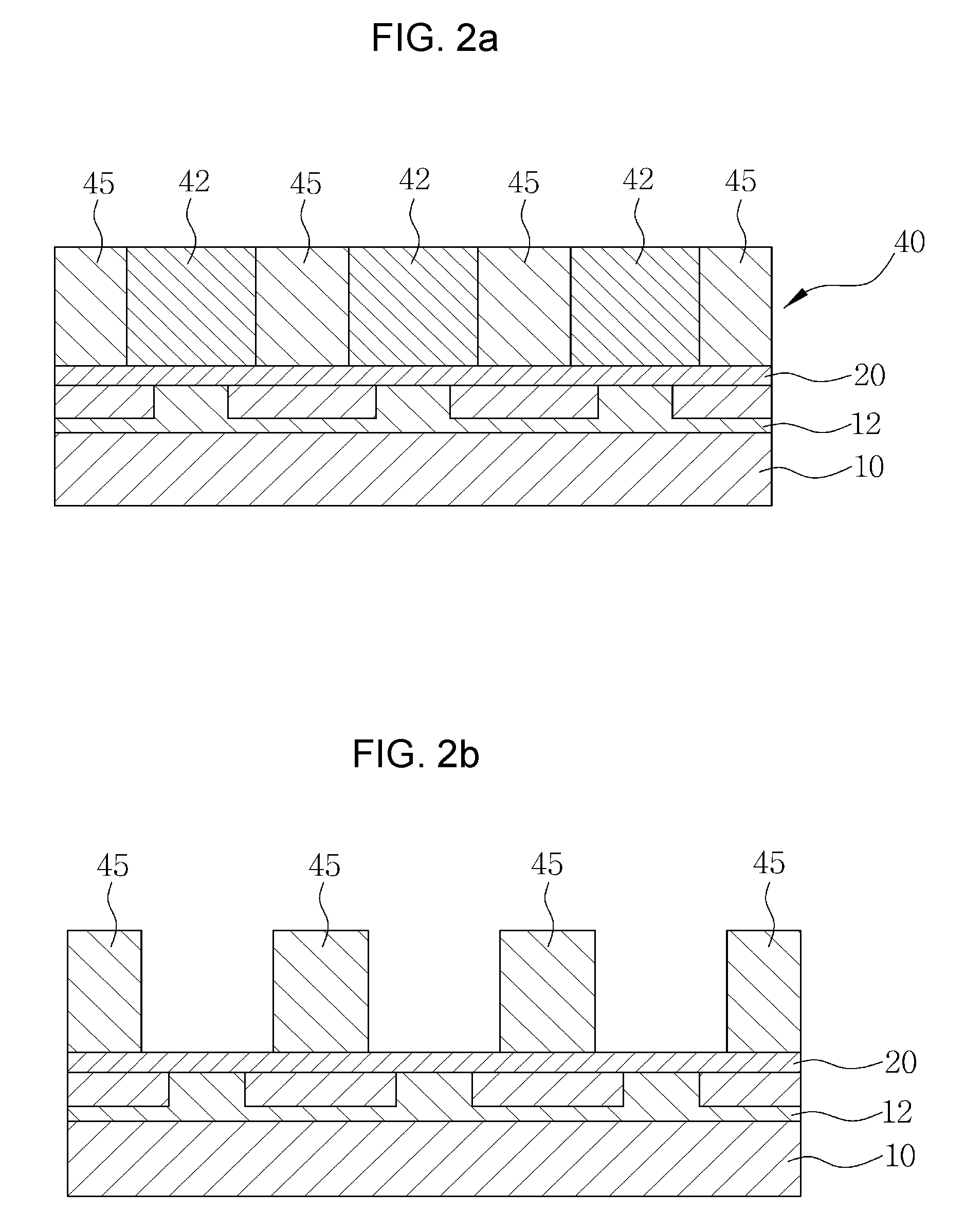
[0038]FIG. 1 is cross sectional view of copper pillar tin bump according to present invention.

[0039]Refer...


PUM

PropertyMeasurementUnit
heightaaaaaaaaaa
heightaaaaaaaaaa
areaaaaaaaaaaa

Abstract

Copper pillar tin bump on semiconductor chip comprises a copper layer composed on chip and a tin layer entirely wrapping whole outer surface of said copper layer. A method for forming of the copper pillar tin bump on semiconductor chip comprises: composing the first copper layer on said chip; applying photoresist to said first copper layer, exposing and developing a part of said photoresist, composing the copper pillar layer at the developed part of photoresist, composing the upper tin layer, removing said photoresist, removing said the first copper layer except disposing place of copper pillar layer, composing side tin layer. The minute pattern makes it possible to form a high density packaging by reducing a pitch of copper pillar tin bump. Signal delay can be reduced by low electric resistance, and underfill can be easily soaked.

Description

CROSS REFERENCE[0001]This application claims foreign priority under Paris Convention and 35 U.S.C. §119 to Korean Patent Application No. 10-2007-0117201, filed Nov. 16, 2007 with the Korean Intellectual Property Office.BACKGROUND OF THE INVENTION[0002]The present invention relates to copper pillar tin bump on semiconductor chip and method of forming of the same, and more particularly, through the simple progress of single photoresist patterning to compose the copper pillar tin bump, it's possible to simplify the progress and reduce the production costs.[0003]Related prior patents are U.S. Pat. No. 7,183,648, USPub. 2006 / 0094226, U.S. Pat. No. 7,122,403, International Application No. PCT / US2004 / 040197.[0004]These days, electronic products has been rapidly developed and it was caused by four factors, techniques of semiconductor designing, semiconductor packaging, semiconductor manufacturing, software programming.[0005]A techniques of semiconductor designing includes composing over mil...

Claims


Application Information

Patent Timeline
Patent Type & Authority Patents(United States)
IPC IPC(8): H01L21/44
CPCH01L24/11H01L2224/13099H01L2224/16H01L2924/01029H01L2924/01078H01L2924/014H01L2924/01082H01L2924/30105H01L2924/01005H01L2924/01006H01L2924/01033H01L2924/01079H01L2224/11825H01L24/13H01L2224/0401H01L2224/05647H01L2224/119H01L2224/13147H01L2224/13562H01L2224/1357H01L2224/13611H01L2224/05568H01L2224/11831H01L2224/0361H01L2224/1147H01L2224/03912H01L24/03H01L24/06H01L24/05H01L2924/00014
Inventor LEE, KANGHONG, SANG JEEN
Owner HWABEAK ENG
Why Eureka
Try Eureka