Design structures for high-voltage integrated circuits

a design structure and integrated circuit technology, applied in the field of semiconductor device fabrication, can solve the problems of large number of fabrication steps, and difficulty in perfecting thick gate oxides in high-performance cmos,

Inactive Publication Date: 2010-08-31
GLOBALFOUNDRIES INC
View PDF48 Cites 196 Cited by
  • Summary
  • Abstract
  • Description
  • Claims
  • Application Information

AI Technical Summary

Problems solved by technology

Thick gate oxides may be difficult to perfect in high-performance CMOS because of the relatively small thickness of the SOI layer.
Moreover, integration of both low-voltage MOSFET devices and high-voltage MOSFET or JFET devices in a single integrated circuit in conventional CMOS fabrication schemes may require a relatively large number of fabrication steps and a large number of different masks as the devices are concurrently fabricated.

Method used


Image

  • Design structures for high-voltage integrated circuits
  • Design structures for high-voltage integrated circuits
  • Design structures for high-voltage integrated circuits

Examples


Embodiment Construction

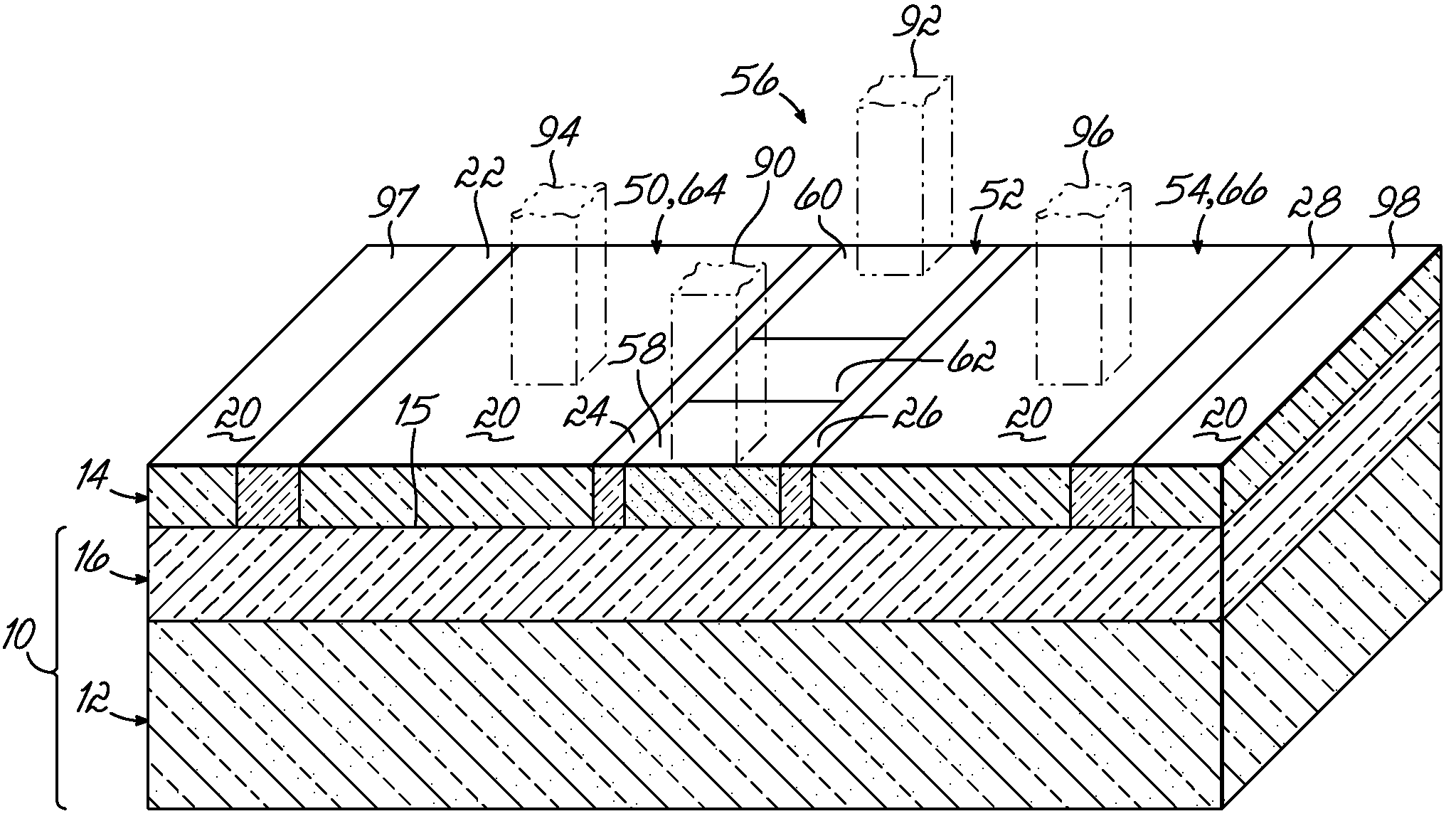
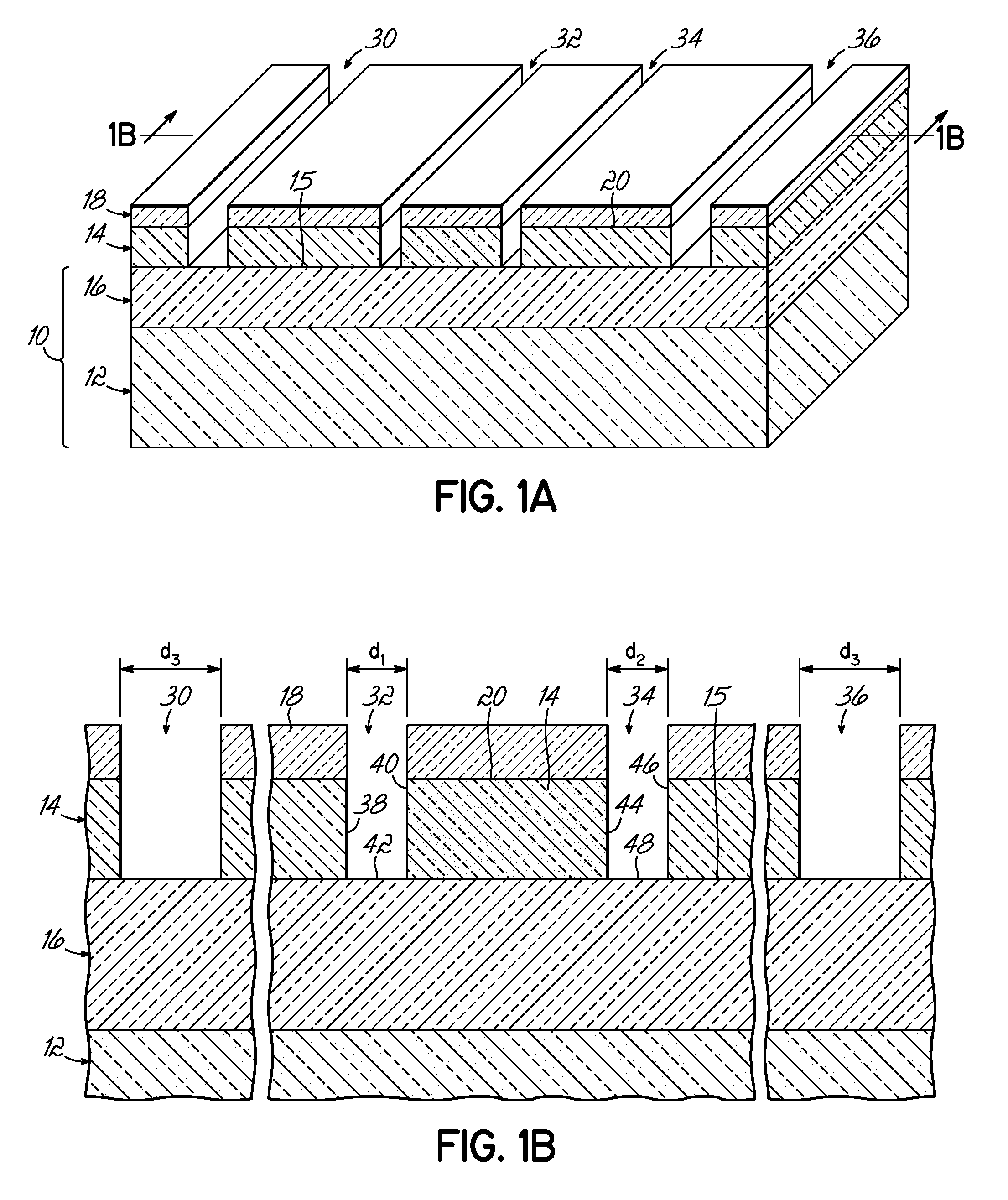
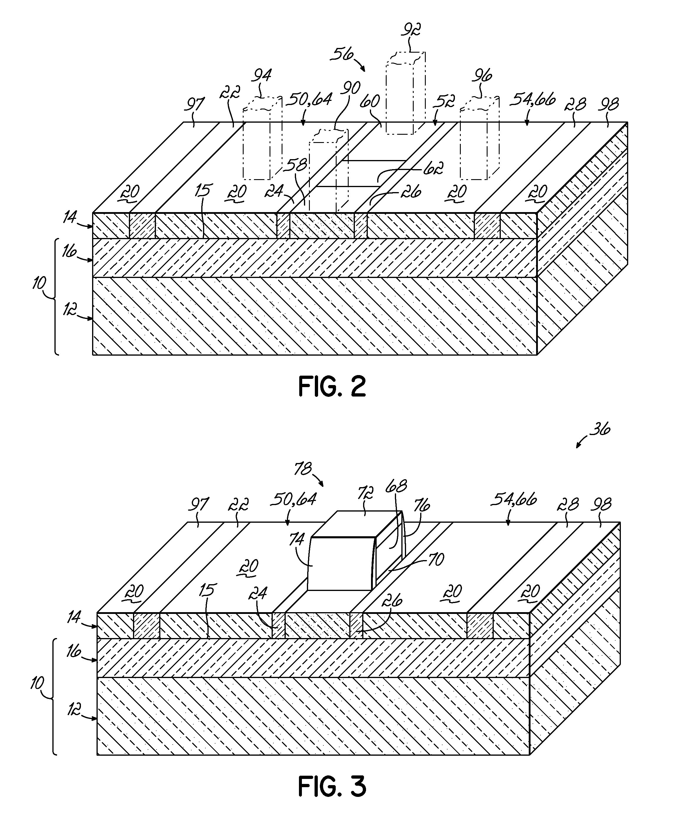
[0017]With reference to FIGS. 1A and 1B and in accordance with an embodiment of the invention, a semiconductor-on-insulator (SOI) substrate 10 includes a handle wafer 12, an active semiconductor or SOI layer 14, and a buried insulating layer 16 formed of an insulating material. The buried insulating layer 16 may be a buried oxide layer containing silicon dioxide (e.g., SiO2). The SOI layer 14 is separated from the handle wafer 12 by the intervening buried insulating layer 16. The SOI layer 14 is composed of single crystal or monocrystalline semiconductor material, such as silicon or a material that primarily contains silicon. The monocrystalline semiconductor material of the SOI layer 14 may contain a definite defect concentration and still be considered single crystal. The handle wafer 12 may also be constituted by a single crystal or monocrystalline semiconductor material, such as silicon, or another type of material. The buried insulating layer 16 electrically isolates the handle...


PUM


Abstract

Design structures for high-voltage integrated circuits. The design structure, which is formed using a semiconductor-on-insulator (SOI) substrate, may include device structure with a semiconductor body positioned between first and second gate electrodes. The first and second gate electrodes and the semiconductor body may be formed from the monocrystalline SOI layer of the SOI substrate. A dielectric layer separates each of the first and second gate electrodes from the semiconductor body. These dielectric layers are formed by defining trenches in the SOI layer and filling the trenches with a dielectric material, which may occur concurrently with a process forming other device isolation regions.

Description

CROSS-REFERENCE TO RELATED APPLICATIONS[0001]This application is a continuation-in-part of application Ser. No. 12 / 013,101, filed Jan. 11, 2008, the disclosure of which is hereby incorporated by reference herein in its entirety.FIELD OF THE INVENTION[0002]The invention relates generally to semiconductor device fabrication and, in particular, to design structures for high voltage integrated circuits.BACKGROUND OF THE INVENTION[0003]Complementary metal-oxide-semiconductor (CMOS) technology is used in microprocessors, static random access memories, and other diverse types of digital logic integrated circuits and analog integrated circuits. Conventional device structures for a planar field effect transistor (FET) fabricated using CMOS technology include a semiconductor layer, a source and a drain defined in the semiconductor layer, a channel defined in the semiconductor layer between the source and drain, and a control gate electrode. The material constituting the gate electrode in such...

Claims


Application Information

Patent Timeline
Patent Type & Authority Patents(United States)
IPC IPC(8): H01L29/78
CPCH01L27/1203
Inventor ABOU-KHALIL, MICHEL J.GAUTHIER, JR., ROBERT J.LEE, TOM C.LI, JUNJUNPUTNAM, CHRISTOPHER S.MITRA, SOUVICK
Owner GLOBALFOUNDRIES INC
Why Eureka
Try Eureka