Wafer translator having a silicon core isolated from signal paths by a ground plane

a ground plane and translator technology, applied in the field of semiconductor test equipment, can solve the problem of not packaging integrated circuits that cannot perform as desired

Active Publication Date: 2010-09-07
TRANSLARITY INC
View PDF3 Cites 22 Cited by
  • Summary
  • Abstract
  • Description
  • Claims
  • Application Information

AI Technical Summary

Problems solved by technology

In this way, integrated circuits that cannot perform as desired are not packaged, or otherwise incorporated into finished products.

Method used


Image

  • Wafer translator having a silicon core isolated from signal paths by a ground plane
  • Wafer translator having a silicon core isolated from signal paths by a ground plane
  • Wafer translator having a silicon core isolated from signal paths by a ground plane

Examples


Embodiment Construction

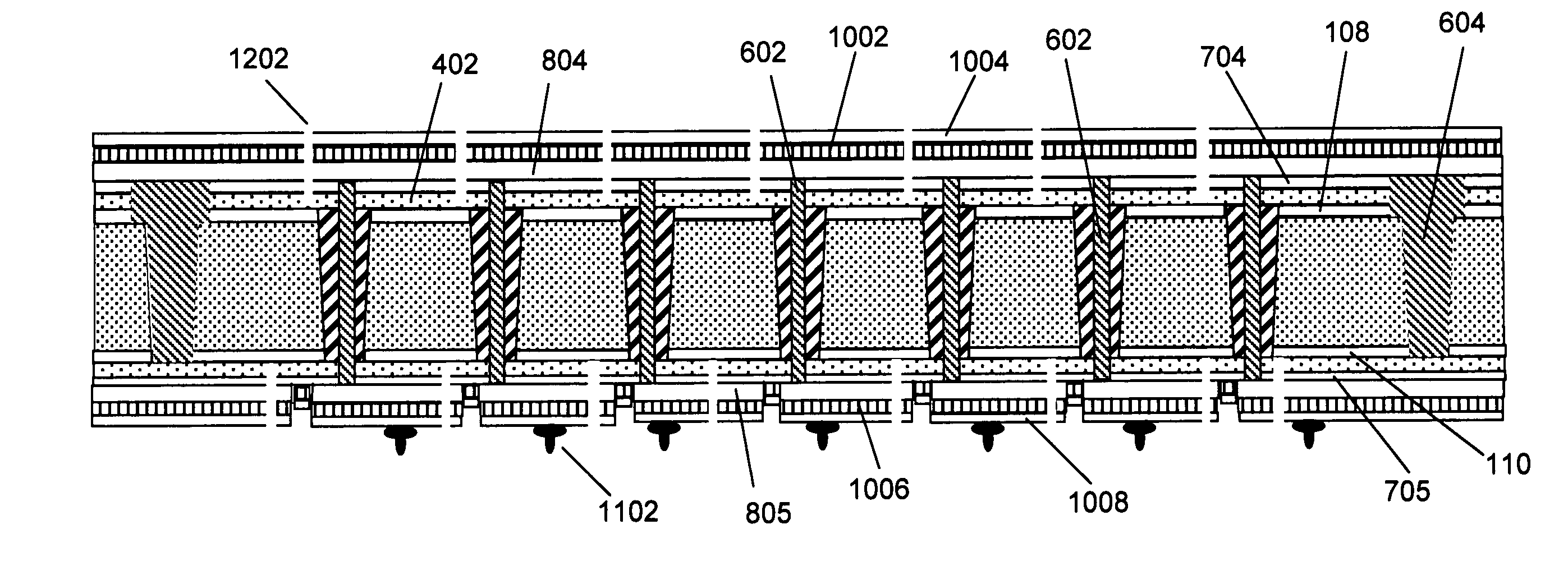
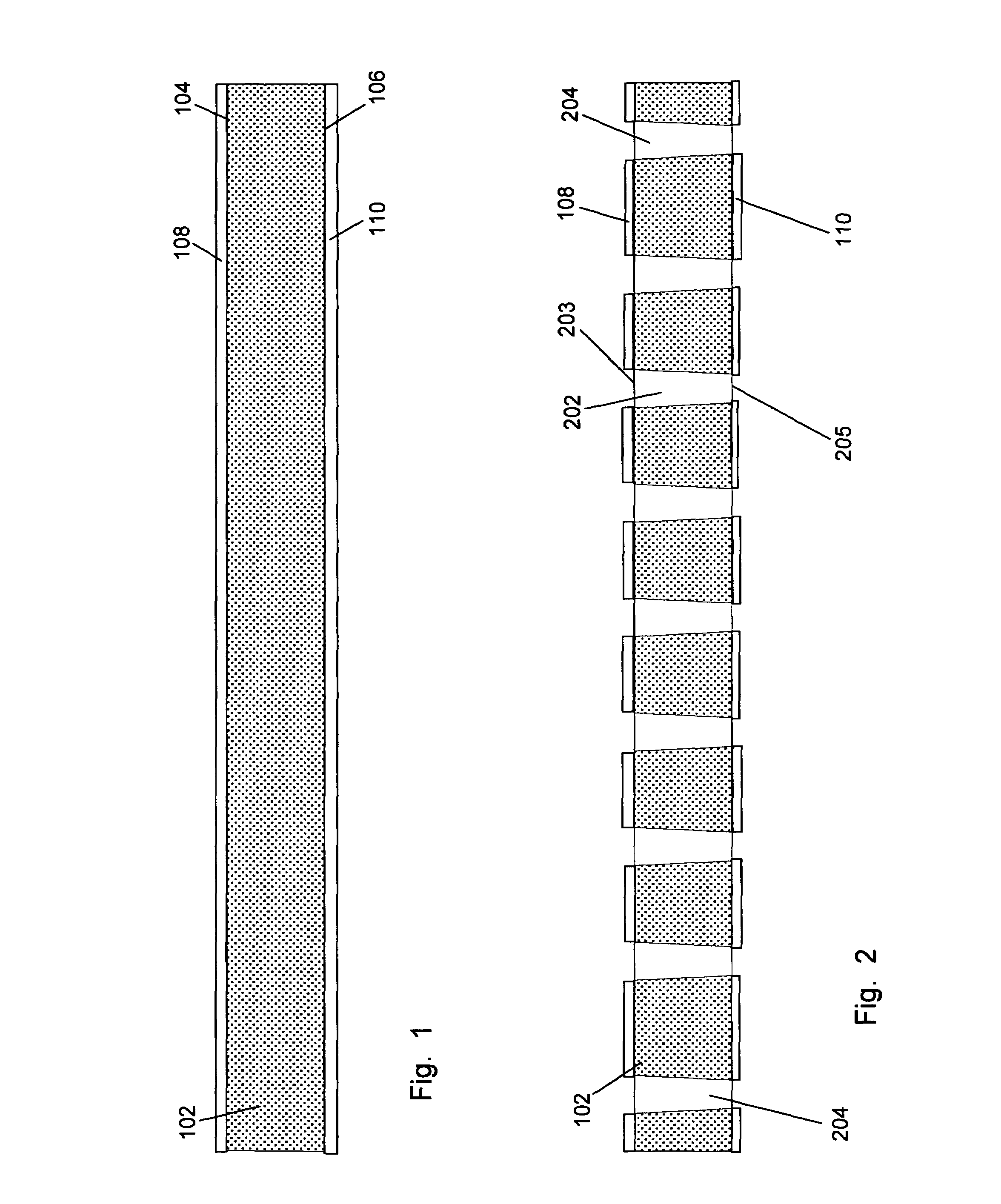
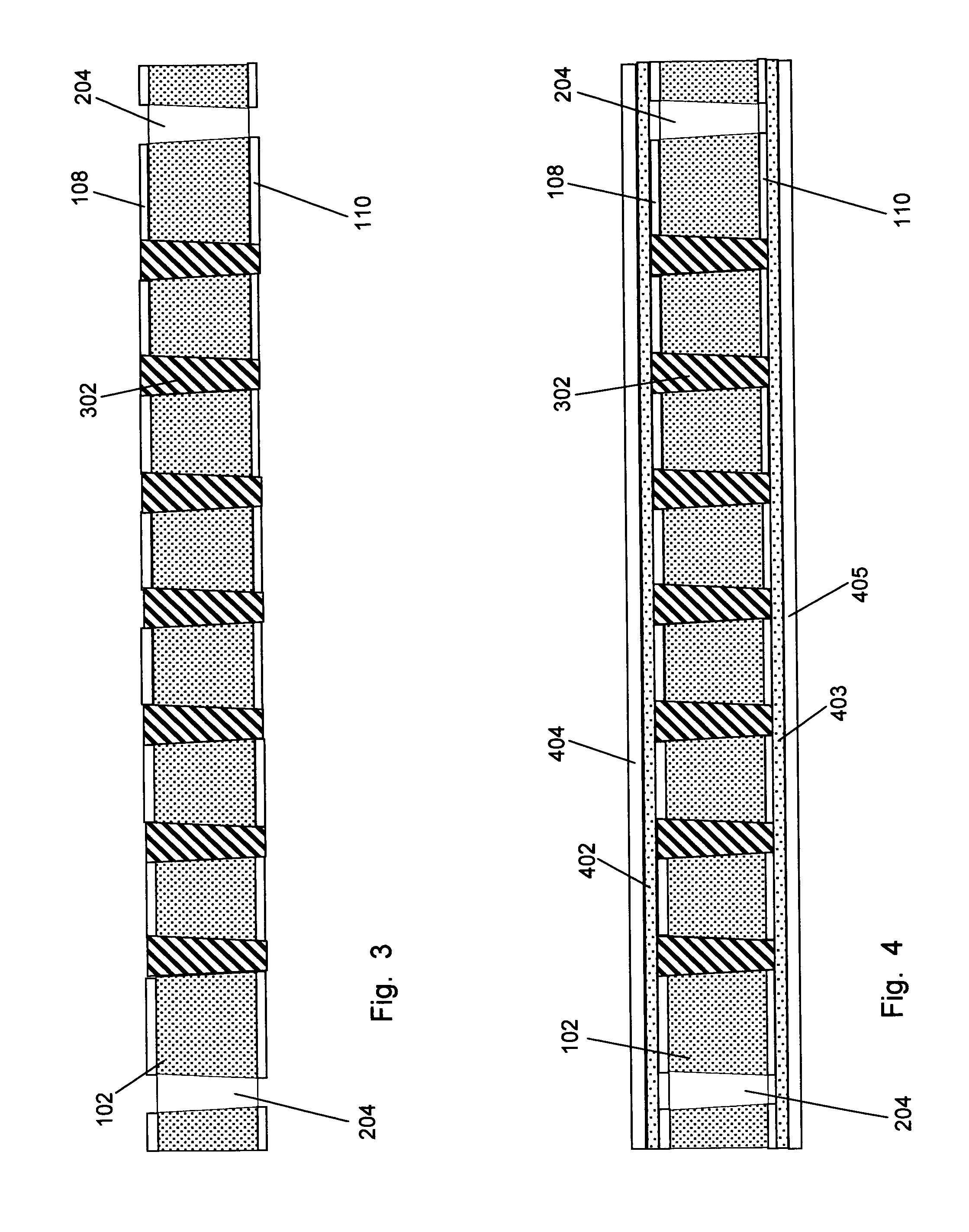
[0029]Generally, a wafer translator (see below for detailed discussion) is formed with processing steps not previously applied to silicon wafers, or substrates, in order to form a unique apparatus having a coefficient of thermal expansion substantially equal to that of a wafer having integrated circuits to be tested, or otherwise operated.

[0030]Reference herein to “one embodiment”, “an embodiment”, or similar formulations, means that a particular feature, structure, operation, or characteristic described in connection with the embodiment, is included in at least one embodiment of the present invention. Thus, the appearances of such phrases or formulations herein are not necessarily all referring to the same embodiment. Furthermore, various particular features, structures, operations, or characteristics may be combined in any suitable manner in one or more embodiments.

Terminology

[0031]Pad refers to a metallized region of the surface of an integrated circuit, which is used to form a p...


PUM

PropertyMeasurementUnit
thicknessaaaaaaaaaa
thicknessaaaaaaaaaa
temperatureaaaaaaaaaa

Abstract

Apparatus and methods are provided for wafer translators having a silicon core, an isolating conductive ground plane, and copper and subjacent resin layers disposed on the ground plane. A silicon substrate having at least one major surface coated with an electrically conductive layer is subjected to a number of printed circuit board manufacturing operations including, but not limited to, application of resin-coated copper foils; mechanical grinding of copper layers; mechanical drilling of via openings in a dielectric material; plating of copper, nickel, and gold layers; laser removal of metal; and chemical removal of metal; in order to produce a wafer translator having a silicon core. In further aspects of the present invention, alignment marks are formed and contact structures, such as stud bumps, are placed relative to a local set of alignment marks.

Description

RELATED APPLICATIONS[0001]This application is a continuation in part of application Ser. No. 12 / 074,904, filed 7 Mar. 2008 now abandoned, and entitled “A Wafer Translator Having A Silicon Core Fabricated With Printed Circuit Board Manufacturing Techniques”, the entirety of which is hereby incorporated by reference.FIELD OF THE INVENTION[0002]The present invention relates generally to semiconductor test equipment, and more particularly relates to methods and apparatus for providing electrical pathways between the pads of integrated circuits on a wafer and circuitry external to the wafer.BACKGROUND[0003]Advances in semiconductor manufacturing technology have resulted in, among other things, reducing the cost of sophisticated electronics to the extent that integrated circuits have become ubiquitous in the modern environment.[0004]As is well-known, integrated circuits are typically manufactured in batches, and these batches usually contain a plurality of semiconductor wafers within and ...

Claims


Application Information

Patent Timeline
Patent Type & Authority Patents(United States)
IPC IPC(8): H01L29/40
CPCH01L21/486H01L21/76898H01L23/481H01L23/49822H01L23/49827Y10T29/49139H01L2924/0002Y10T29/49126H01L2924/00H01L2924/00012G01R1/07342
Inventor JOHNSON, MORGAN T.
Owner TRANSLARITY INC
Why Eureka
Try Eureka