Semiconductor device and method of manufacturing the same

a semiconductor and semiconductor technology, applied in semiconductor devices, semiconductor/solid-state device details, electrical apparatus, etc., can solve the problems of reducing the parasitic capacitance of the inter-wiring, increasing the density of the wiring pattern, and increasing the parasitic capacitance generated between wires, so as to reduce the total interlayer insulation film, reduce the signal delay on the wiring, and improve the signal delay characteristics of the wiring

Active Publication Date: 2010-09-14
PANNOVA SEMIC
View PDF5 Cites 7 Cited by
  • Summary
  • Abstract
  • Description
  • Claims
  • Application Information

AI Technical Summary

Benefits of technology

[0019]The present invention has been made to solve the conventional problems described above, and an object of the present invention is to provide a semiconductor device including a metallic wire covered by a low-permittivity film and a method of manufacturing the same, wherein the semiconductor device is capable of: suppressing an increase in the permittivity of an entire first insulation film; suppressing an increase in the relative permittivity of a low permittivity film on wall faces and bottom faces of a wiring groove and a via hole; reducing signal delay on the wiring; and improving signal delay characteristics on the wiring until a desired state is reached.
[0025]Moreover, a method of manufacturing a semiconductor device according to the present invention includes the steps of: (a) forming a via hole on an interlayer insulation film formed on a substrate; (b) forming a wiring groove on the interlayer insulation film after the step (a); (c) covering lateral walls and bottom portions of the via hole and the wiring groove with an inside-face insulation film after the step (b); (d) covering, via the inside-face insulation film, the lateral walls and bottom portions of the via hole and the wiring groove with a barrier metal film after the step (c); and (e) lowering the permittivity of the inside-face insulation film after the step (d).
[0026]Furthermore, in the method of manufacturing a semiconductor device described above, the permittivity of the interlayer insulation film is lowered in comparison to the permittivity of the inside-face insulation film formed in the step (c).
[0027]Furthermore, in the method of manufacturing a semiconductor device described above, the permittivity of the inside-face insulation film is lowered to substantially 2.5 or lower in the step (e).
[0033]Consequently, an effect can be achieved where the effective permittivity between the wires is lowered, the signal delay on the wiring is reduced, and signal delay characteristics on the wiring can be improved to a desired state.
[0035]Consequently, an effect can be achieved where the permittivity of the entire interlayer insulation film is lowered, signal delay on the wiring is reduced, and signal delay characteristics on the wiring can be improved to a desired state.

Problems solved by technology

The increasingly higher integration of semiconductor integrated circuits in recent years has led to higher density in wiring patterns and, in turn, an increase in a parasitic capacitance generated between wires.
Since such an increase in the parasitic capacitance causes signal wiring delay, reducing the inter-wiring parasitic capacitance is an important issue in semiconductor integrated circuits that must be operated at high speed.
However, when using a low-permittivity film made up of SiOC or porous SiOC as an insulation film between wires, the high proportion of Si—CH3 bonds / Si—O bonds in the film causes the Si—CH3 bonds to be separated by plasma processing performed during a barrier metal film formation process or the like, resulting in an increase in high-dielectric Si—O bonds.
As a result, the relative permittivity of the SiOC film disadvantageously increases.
As a result, signal delay on the wiring increases.
In addition, since the pore seal film contains Si—CH3 bonds and is therefore vulnerable to plasma processing, the Si—CH3 bonds in the low-permittivity film on the wall faces and bottom faces of the wiring groove and the via hole are separated by plasma processing applied to the wiring groove and the via hole during the barrier metal film formation process or the like.
As a result, relative permittivity increases which, in turn, causes degradation of signal delay characteristics on the wiring.

Method used


Image

  • Semiconductor device and method of manufacturing the same
  • Semiconductor device and method of manufacturing the same
  • Semiconductor device and method of manufacturing the same

Examples


Embodiment Construction

[0059]Hereinafter, a semiconductor device and a method of manufacturing the same representing an embodiment of the present invention will be specifically described with reference to the drawings.

[0060]Further, materials and numeric values used in the present invention are preferable examples but are not restrictive. The materials and numeric values can be appropriately changed without departing from the scope of the invention.

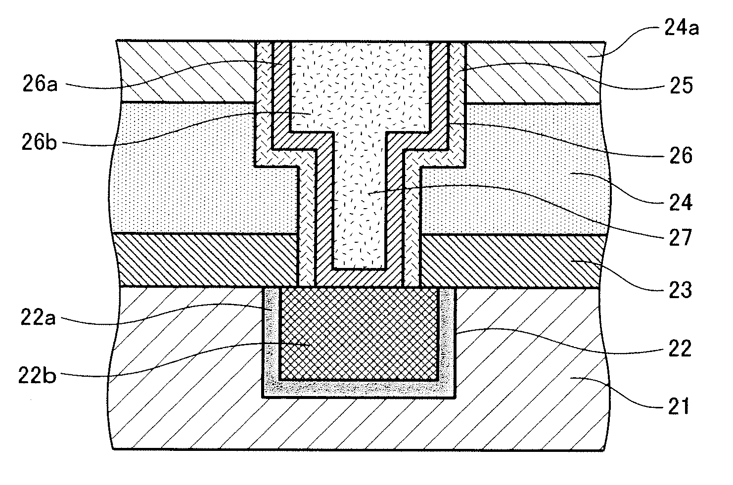
[0061]FIG. 3 shows a cross-sectional structure of a wiring portion of a semiconductor device according to the present embodiment. As shown in FIG. 3, a first metallic wire 22 is formed on a first insulation film 21 composed of silicon dioxide (SiO2) and formed on top of a substrate (not shown) composed of Si by a barrier metal film 22a composed of tantalum nitride (TaN) and a conductive film 22b composed of copper (Cu). A second insulation film 23 composed of silicon carbide (SiC) and which functions as an anti-metallic diffusion film is formed on top of the fi...


PUM


Abstract

By covering inner surfaces of a wiring groove 26c and a via hole 27a with a fourth insulation film 25 containing porogen during a manufacturing process of a semiconductor device, an increase in the relative permittivity of the fourth insulation film 25 that is a low-permittivity film on the inner surfaces of the wiring groove 26c and the via hole 27a can be suppressed in a manufacturing process of a semiconductor device such as a barrier metal sputtering process.

Description

FIELD OF THE INVENTION[0001]The present invention relates to a semiconductor device provided with metallic wiring composed of copper or the like and a low-permittivity interlayer insulation film, and a method of manufacturing the same.BACKGROUND OF THE INVENTION[0002]The increasingly higher integration of semiconductor integrated circuits in recent years has led to higher density in wiring patterns and, in turn, an increase in a parasitic capacitance generated between wires. Since such an increase in the parasitic capacitance causes signal wiring delay, reducing the inter-wiring parasitic capacitance is an important issue in semiconductor integrated circuits that must be operated at high speed. Currently, reduction in the inter-wiring parasitic capacitance is realized by reducing the relative permittivity between wires and of interlayer insulation films.[0003]Conventionally, a silicon dioxide film (SiO2) (relative permittivity of substantially 3.9 to 4.2) or a SiO2 film containing f...

Claims


Application Information

Patent Timeline
Patent Type & Authority Patents(United States)
IPC IPC(8): H01L21/4763
CPCH01L21/7682H01L21/76822H01L21/76825H01L21/76829H01L21/76831H01L21/76835H01L23/5226H01L23/53238H01L23/53295H01L21/76807H01L2924/0002H01L2924/00H01L2221/1047
Inventor NOMURA, KOTARO
Owner PANNOVA SEMIC
Why Eureka
Try Eureka