Hierarchical module

a hierarchy module and module technology, applied in the field of memory modules, can solve the problems of difficult capacity increase and cost increase, and achieve the effects of high speed transfer rate, convenient optimal wiring, and large capacity

Inactive Publication Date: 2010-09-21
RENESAS ELECTRONICS CORP
View PDF28 Cites 9 Cited by
  • Summary
  • Abstract
  • Description
  • Claims
  • Application Information

AI Technical Summary

Benefits of technology

[0020]Therefore, there is much desired in the art for a module architecture that realizes a system where it is possible to parallel-dispose multiple modules, increase the transfer rate speed, and handle large capacity.
[0033]According to the present invention, a system with a high-speed transfer rate and large capacity can be realized by employing the hierarchical module architecture comprising the second module that facilitates an optimum wiring between the first modules and the controller circuit.
[0034]According to the present invention, the difficulty in wiring design of the motherboard 40 is eliminated by employing the structure where the first modules are mounted on the second module and not directly on the motherboard.
[0035]According to the present invention, the data transfer speed of each pin can be improved greatly by employing the hierarchical module architecture, and the test cost, development cost, and power consumption of the pins at the same data rate can be reduced.
[0036]According to the present invention, even when the number of the modules connected is increased, the increase in latency can be restrained.

Problems solved by technology

For instance, if eight of the first modules are parallel-connected, the motherboard will require not less than eight layers, resulting in a cost increase.
Therefore, it is difficult to increase capacity.

Method used


Image

  • Hierarchical module
  • Hierarchical module
  • Hierarchical module

Examples


embodiment

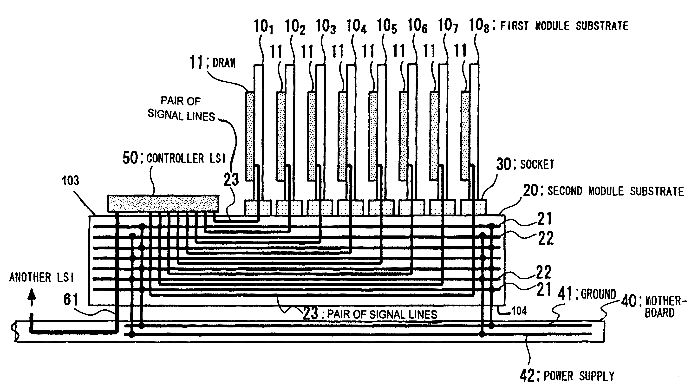
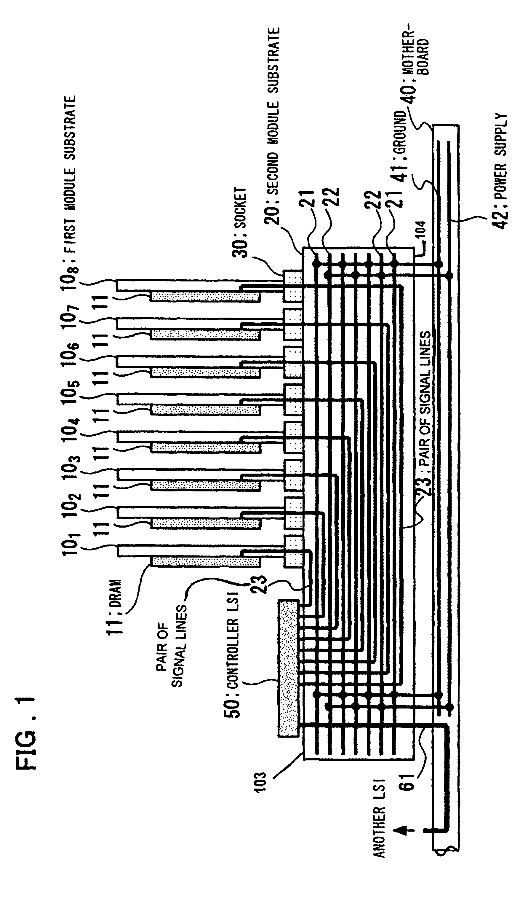
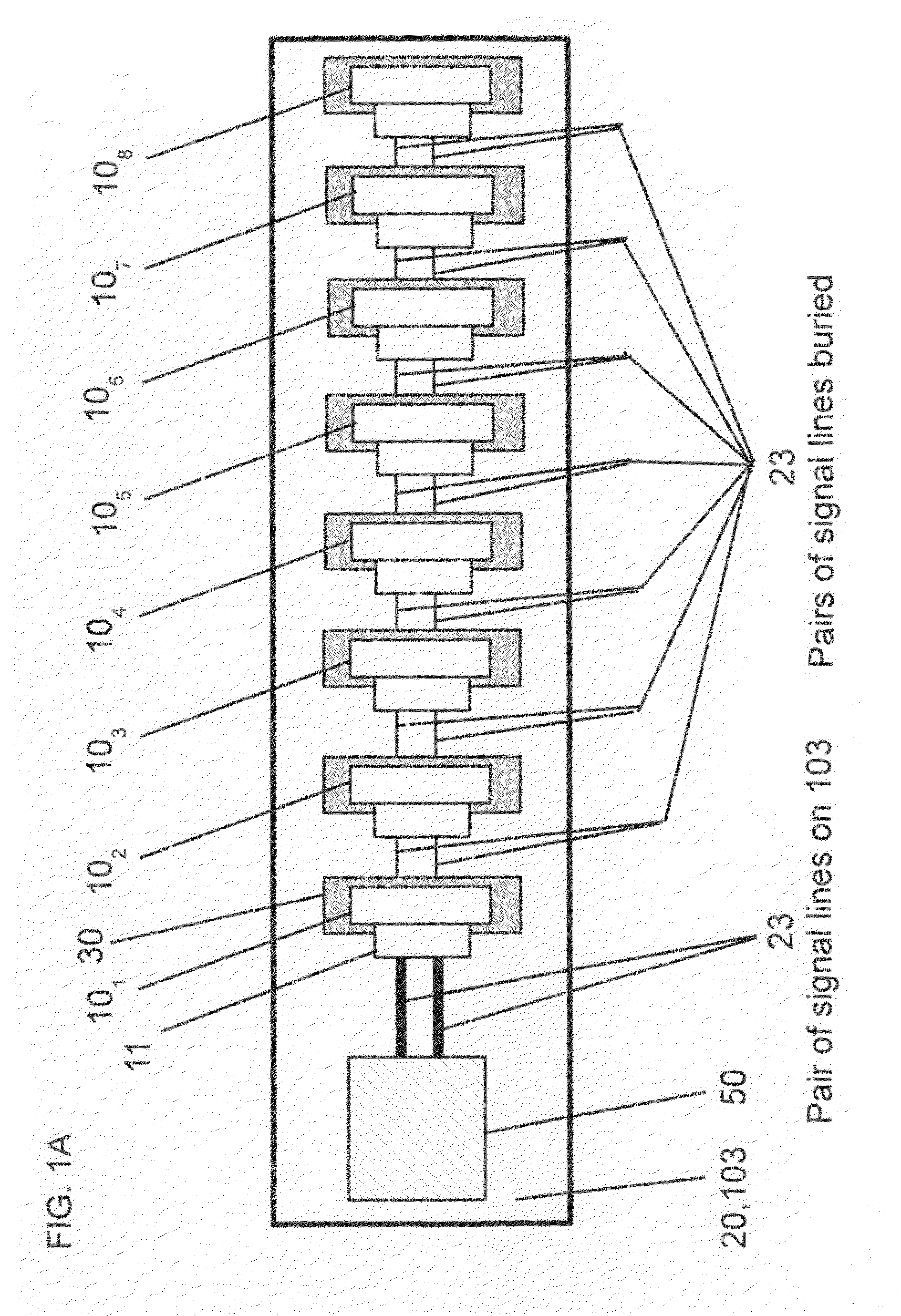
[0044]FIGS. 1 and 1A are drawings showing the structure of a first embodiment of the present invention. In reference to FIGS. 1 and 1A, in the first embodiment of the present invention, the first module substrates 10 with the DRAMs 11 has the same structure (DIMM) as the first module substrates 10 described with reference to FIGS. 5 and 6, the first module substrates 10 are inserted into sockets 30 and mounted on the second module substrate 20. The sockets 30 are soldered and fixedly connected to the second module substrate 20. The second module substrate 20 is connected on the motherboard 40 by soldering, for example.

[0045]In the present embodiment, the controller LSI 50 such as a DRAM controller is mounted on the second module substrate 20 as well, and the sockets 30, into which each of the eight first module substrates 101 to 108 are inserted, and the corresponding pins (electrodes) of the controller LSI 50 are connected in parallel to each other by the pairs of wiring lines (sig...


PUM


Abstract

There is provided a memory module that facilitates meeting the needs of high-speed performance and large capacity. It comprises first module substrates (101 through 108), each with multiple DRAM devices (11), and a second module substrate whereon the first modules (101 through 108) are mounted, signal line groups connected to the multiple first modules respectively are provided in parallel, and a controller LSI (50), connected to the multiple first modules respectively via the signal line groups provided in parallel, that converts the signal lines into fewer signal lines than the total number of the signal line groups and outputs the result is provided, and the second module substrate (20) is mounted on a motherboard (40).

Description

FIELD OF THE INVENTION[0001]The present invention relates to a memory module and especially to a hierarchical module architecture that facilitates coping with high-speed performance.BACKGROUND OF THE INVENTION[0002]A DIMM (Dual Inline Memory Module) has card edge connectors for transmitting and receiving electric signals externally where electric signals are assigned to the front and back of the board (one row each), and various kinds of products such as DDR (Double Data Rate), SDRAM (Synchronous DRAM), and 184-pin DIMM (400 MHz / 256 MB) have been on the market. A DIMM is used for PCs and workstations, for instance, and mounted on the board perpendicularly using a DIMM socket.[0003]FIG. 5 is a drawing showing an example of the structure of a conventional memory module (multidrop system). In reference to FIG. 5, first module substrates 10, each of which has multiple DRAMs 11 (eight of them, for example), are inserted into sockets 30 soldered to a motherboard 40. In the example shown i...

Claims


Application Information

Patent Timeline
Patent Type & Authority Patents(United States)
IPC IPC(8): H05K1/11H05K1/14G06F13/16G06F12/00G11C5/06G11C7/00H05K3/36
CPCG06F13/1684G11C5/04G11C5/066H05K1/14Y02B60/1228H05K3/366H05K2201/045H05K2201/10159H05K1/141Y02D10/00G06F12/00G11C11/407
Inventor SAEKI, TAKANORI
Owner RENESAS ELECTRONICS CORP
Why Eureka
Try Eureka