Method for manufacturing semiconductor device

Inactive Publication Date: 2010-10-05
SK HYNIX INC
View PDF1 Cites 4 Cited by
  • Summary
  • Abstract
  • Description
  • Claims
  • Application Information

AI Technical Summary

Benefits of technology

[0026]Embodiments of the present invention are directed to a method for manufacturing a semiconductor device that can reduce the thickness o

Problems solved by technology

However, in the case of increasing the height of the capacitor so as to secure desired capacitance of the capacitor, problems are caused due to an increase in the depth of step portions, resulting from the increase in the height of the capacitor.
Further, in the case of reducing the thickness of a dielectric layer, leakage current increases.
However, the above-described conventional method for manufacturing a semiconductor device has the

Method used


Image

  • Method for manufacturing semiconductor device
  • Method for manufacturing semiconductor device
  • Method for manufacturing semiconductor device

Examples


Example

[0040]As required, detailed embodiments of the present invention are disclosed herein. However, it is to be understood that the disclosed embodiments are merely exemplary of the invention, which may be embodied in various forms. Therefore, specific details disclosed herein are not to be interpreted as limiting, but merely as a basis for the claims and as a representative basis for teaching one skilled in the art to variously employ the present invention in virtually any appropriate manner.

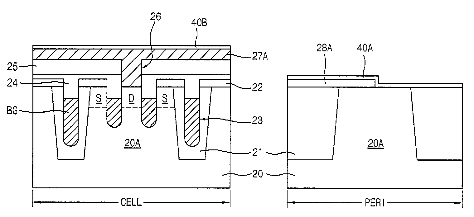
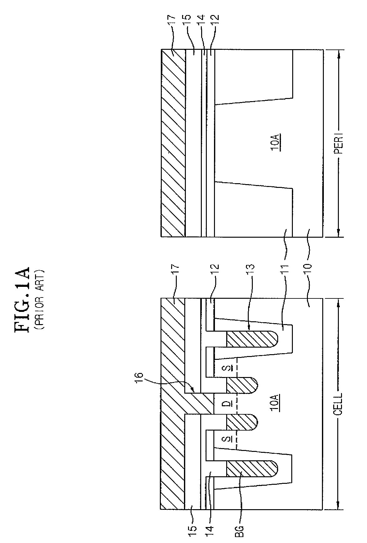
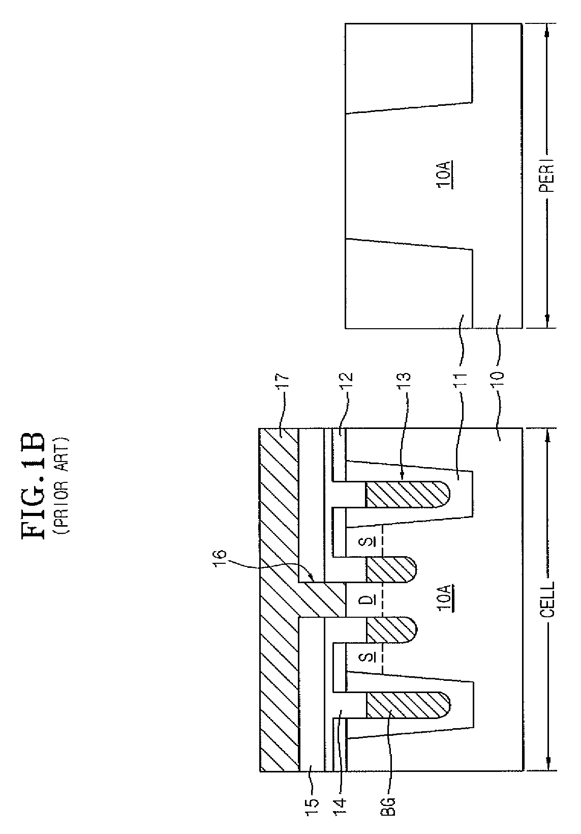
[0041]In the present approach, the thickness of an oxide layer formed on a polysilicon layer for bit line contacts is reduced. Through this, in the present approach, it is possible to prevent the occurrence of a short-circuit between adjoining bit lines due to the oxide layer.

[0042]In the present approach, due to the fact that the thickness of the oxide layer is reduced, it is not necessary to conduct overetching in a subsequent etching process. Accordingly, in the present approach, it is possible ...


PUM


Abstract

Methods for manufacturing a semiconductor device are provided that reduces the thickness of an oxide layer formed on a polysilicon layer for bit line contacts. A reduced thickness oxide layer can prevent short circuits between adjoining bit lines. A reduced thickness oxide layer can also eliminate the need for overetching in a subsequent etching process, thereby preventing loss of an isolation layer in a peripheral region.

Description

CROSS-REFERENCE TO RELATED APPLICATIONS[0001]The present application claims priority to Korean patent application number 10-2009-0057524 filed on Jun. 26, 2009, which is incorporated herein by reference in its entirety.BACKGROUND OF THE INVENTION[0002]The present invention generally relates to a method for to manufacturing a semiconductor device, and more particularly, to a method for manufacturing a semiconductor device that can reduce the thickness of an oxide layer formed on a polysilicon layer for bit line contacts.[0003]In a DRAM (dynamic random access memory) in which a is unit cell is constituted by one MOS (metal oxide semiconductor) transistor and one capacitor, it is important to have a high degree of integration in order to increase the capacitance of the capacitor that occupies a large area, and decrease the area that is occupied by the capacitor.[0004]Therefore, in order to form a capacitor having high capacitance within a small area, attempts such as increasing the hei...

Claims


Application Information

Patent Timeline
IPC IPC(8): H01L21/82
CPCH01L27/10888H01L27/10894H10B12/485H10B12/09H01L21/18H10B99/00
Inventor KIM, HYUNG KYUNJOUNG, YONG SOO
Owner SK HYNIX INC
Why Eureka
Try Eureka