Semiconductor device, unique ID of semiconductor device and method for verifying unique ID

a semiconductor device and unique id technology, applied in the field of semiconductor devices, can solve the problems of plurality of same unique ids accidentally, long manufacturing time of semiconductor devices such as socs, and difficulty in recording them in memory mounted on normal cmos, etc., to achieve excellent uniqueness, easy verification, and shorten manufacturing time

Inactive Publication Date: 2010-10-05
RENESAS ELECTRONICS CORP
View PDF17 Cites 2 Cited by
  • Summary
  • Abstract
  • Description
  • Claims
  • Application Information

AI Technical Summary

Benefits of technology

[0020]It is a first object of the present invention to provide a semiconductor device whose manufacturing time can be shortened. In addition, it is a second object of the present invention to provide a unique ID of a semiconductor device that is excellent in uniqueness and can be easily verified.
[0022]Therefore, the number of laser trimming performed in recording data can be reduced. Thus, the manufacturing time can be shortened.
[0024]As described above, since the unique ID comprises the unique chip information containing the information of the manufactured semiconductor device and the inspection bit provided by executing the cyclic redundancy checking operation for the chip information, its uniqueness can be enhanced and its random nature can be also enhanced as compared with the case where the unique ID comprises only the chip information. In addition, it is difficult to decode the information as compared with the case where the unique ID comprises only the chip information, so that the information a semiconductor manufacturer does not want an end user to know is prevented from being disclosed.
[0026]As described above, since the whole unique ID can be verified only by verifying the inspection bit of the cyclic redundancy checking operation in the tester, it can be easily verified whether the unique ID in each chip is defective or not.
[0028]As described above, since the whole unique ID can be verified only by verifying the inspection bit of the cyclic redundancy checking operation by the processing unit in the semiconductor device, it can be easily verified whether the unique ID in each chip is defective or not. Furthermore, since only the information of the compared result is sent to the tester, the number of pins for testing can be reduced.

Problems solved by technology

Although this unique ID can be recorded in a flash ROM (Read Only Memory) and a HDD (Hard Disk Drive) that constitute a system using the above SOC, it is difficult to record it in a memory mounted on a SOC manufactured by a normal CMOS (Complementary Metal Oxide Semiconductor) process.
Thus, the problem is that the manufacturing time of the semiconductor device such as the SOC becomes long.
In addition, although the chip information of the target SOC is used in order to implement a secure function in the unique ID in general, since the chip information has regularity and lacks in random nature, when the fuse is broken unexpectedly or worn out, there generated a plurality of same unique IDs accidentally.
In this case, even when the unique ID is used for implementing the secure function, the secure function cannot be implemented.
Furthermore, since yield information and the like can be guessed from the chip information, the problem is that the information that a SOC manufacturer does not want an end user to know is disclosed.
However, there is the following problem in a case where the unique ID is constituted with data other than the chip information.
That is, in a case where the unique ID comprises random data with respect to each SOC, for example, when the unique ID is verified, it is necessary to prepare the same data as that of the unique ID in a tester as expectation value data to be compared and it is necessary to prepare the expectation value data corresponding to the number of the SOCs in the tester, which takes a lot of trouble.
In addition, since the expectation value is tested in the same function pattern in the test of the LSI in general, when the kinds of the expectation value is increased, it is necessary to prepare the test patterns so as to correspond the number of kinds, which takes a lot of trouble.
In addition, although the test pattern can be incremented every LSI based on one kind of test pattern, this is not practical because the setting of an initial value becomes complicated and it takes a lot of trouble at the time of retesting.

Method used


Image

  • Semiconductor device, unique ID of semiconductor device and method for verifying unique ID
  • Semiconductor device, unique ID of semiconductor device and method for verifying unique ID
  • Semiconductor device, unique ID of semiconductor device and method for verifying unique ID

Examples


embodiment 1

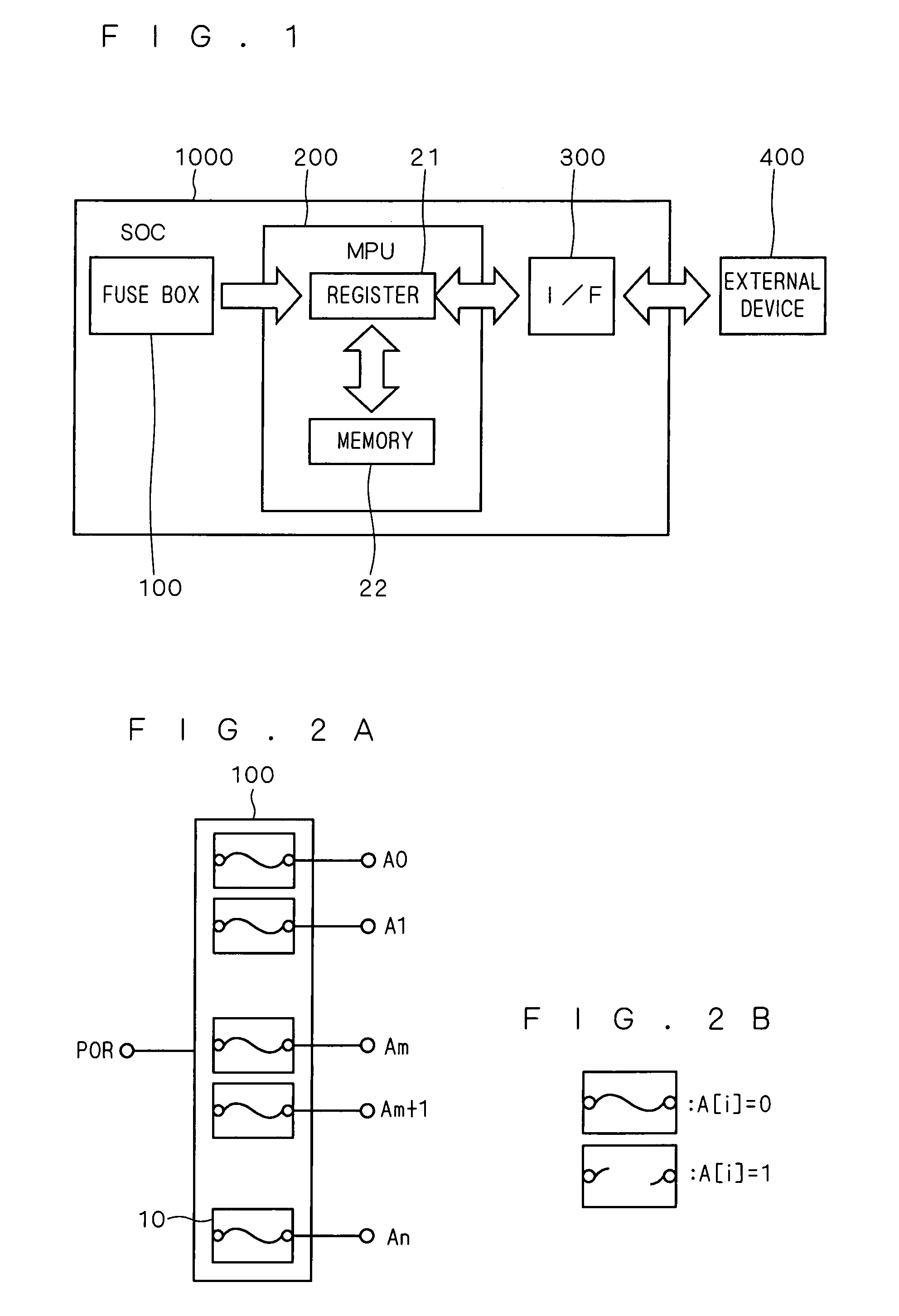
[0048]FIG. 1 is a block diagram showing the constitution of a SOC (System on Chip) 1000 according to an embodiment 1.

[0049]As shown in FIG. 1, the SOC 1000 comprises a fuse box 100, a MPU (Micro Processing Unit) 200 (processing unit) and an I / F (interface) unit 30. The fuse box 100 has a plurality of fuses (not shown in FIG. 1) for recording a unique ID, and each fuse corresponds to each bit of the unique ID. The MPU 200 has a register 21 and a memory 22.

[0050]Referring to FIG. 1, the unique ID recorded in the fuse box 100 is read by the register 21 of the MPU 200 and transferred to an external device 400 through the I / F unit 300. Alternatively, it may be such that the unique ID read by the register 21 is transferred from the register 21 to the memory 22 and stored and processed there and read by the register 21 again and transferred to the external device 200 through the I / F unit 300.

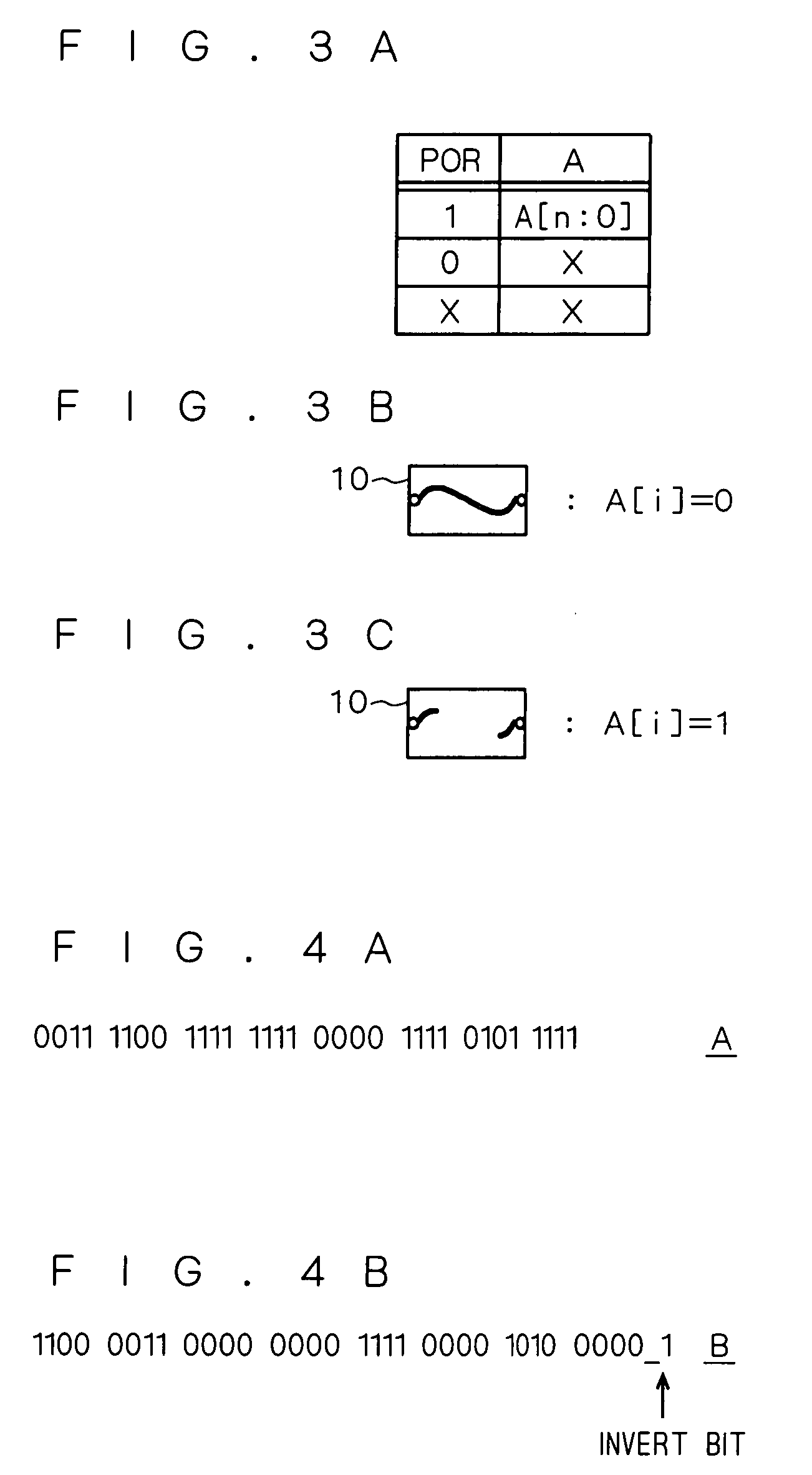
[0051]FIG. 2A is a view schematically showing the fuse box 100 in which the unique ID is recorded o...

embodiment 2

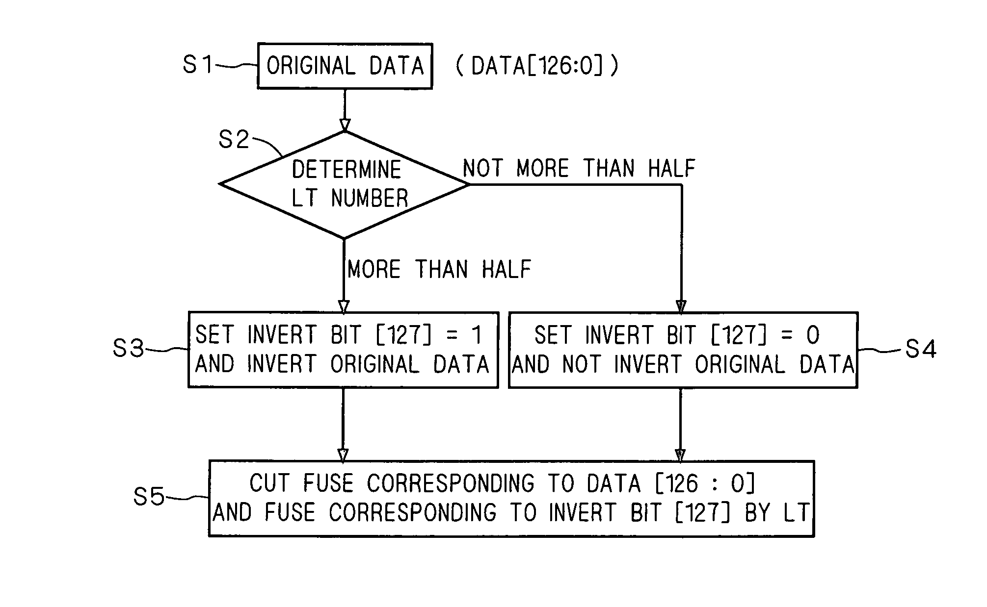
[0083]The description has been made of the case where one invert bit is set for the entire data comprising one bit string in the embodiment 1. However, data used actually include a part in which the ratio of the bit of “1” is extremely small in some cases and in this case, the LT number can be further reduced by removing such part from the object of the invert bit. That is, one invert bit may be set to only a part of the data comprising one bit string.

[0084]FIG. 8 is a flowchart showing steps (unique ID recording steps) of a manufacturing method of a semiconductor device according to an embodiment 2. Referring to FIG. 8, a bit [n] is provided as an invert bit for a bit string [n−1:0] of data having a n-bit length. This bit string [n−1:0] is divided into a bit string [m−1:0] having m-bit length and a bit string [n−1:m] having a (n-m)-bit length (m is a natural number not more than (n−1)), and the invert bit [n] is set only for the bit string [n−1:m]. That is to say, according to the ...

embodiment 3

[0090]The description has been made of the case where one invert bit is set for the data comprising one bit string in the embodiment 2. However, the present invention is not limited to this. For example, two or more invert bits may be set for data comprising one bit string.

[0091]FIG. 9 is a flowchart showing steps (unique ID recording steps) of a manufacturing method of a semiconductor device according to the embodiment 3. Referring to FIG. 9, invert bits [n−1] and [n] are set for a bit string [n−2:0] of data having a (n−1)-bit length. It is assumed that the bit string [n−2:0] is divided into a bit string [k−1:0] having a k-bit length, a bit string [m−1:k] having a (m−k)-bit length, and a bit string [n−2:m] having a (n−m−1)-bit length (k is a natural number not more than (m−1)), and the invert bit [n−1] is set only for the bit string [m−1:k] and the invert bit [n] is set only for the bit string [n−2:m]. That is to say, according to the flowchart in FIG. 9, steps S1 to S4 in the flow...


PUM


Abstract

The present invention relates to a semiconductor device, a unique ID of the semiconductor device and a method for verifying the unique ID. Thus, original data (bit string) having 127-bit length [126:0] is inputted at step S1. Then, it is determined whether the number of bits of “1” in the bit string [126:0] inputted at the step S1 is more than the half of the bits of the bit string (that is, not less than 64) or not at step S2. When the number is not less than 64, the process proceeds to step S3. At the step S3, the bit string [126:0] is inverted and an invert bit [127] is set to “1”. Then, the process proceeds to step S5. At the step S5, the fuse corresponding to the bit string [126:0] and the bit [127] are cut by LT.

Description

BACKGROUND OF THE INVENTION[0001]1. Field of the Invention[0002]The present invention relates to a semiconductor device, a unique ID of the semiconductor device and a method for verifying the unique ID and more particularly, to a technique for shortening a manufacturing time in a SOC (System on Chip) having fuse cutting type of data recording means and a unique ID recorded in a fuse.[0003]2. Description of the Background Art[0004]Conventionally, there is a method for recording a unique identification number, that is, a unique ID uniquely allocated to each SOC (System on Chip) in order to implement a secure function in the SOC (for example, Japanese Patent Application Laid-Open No. 2003-101527).[0005]Although this unique ID can be recorded in a flash ROM (Read Only Memory) and a HDD (Hard Disk Drive) that constitute a system using the above SOC, it is difficult to record it in a memory mounted on a SOC manufactured by a normal CMOS (Complementary Metal Oxide Semiconductor) process. T...

Claims


Application Information

Patent Timeline
Patent Type & Authority Patents(United States)
IPC IPC(8): G01R31/28G11C29/00
CPCG06F21/73G11C7/20G11C17/143G11C17/18G11C29/027G11C29/028G11C2029/4402G11C29/00
Inventor MORI, YASUFUMIAZUMA, KATSUHIKOMIURA, MANABU
Owner RENESAS ELECTRONICS CORP
Why Eureka
Try Eureka