Production method of substrate for liquid crystal display using image-capturing and reference position detection at corner of pixel preset in TFT substrate

a production method and liquid crystal display technology, applied in the field of production methods of substrates for liquid crystal display, can solve the problems of overlapping precision, difficult positioning of each pattern, and difficult miniaturization of pixel regions, so as to suppress the cost increase of the imaging unit and improve the speed of data processing

Inactive Publication Date: 2010-10-12
V TECH CO LTD
View PDF13 Cites 31 Cited by
  • Summary
  • Abstract
  • Description
  • Claims
  • Application Information

AI Technical Summary

Benefits of technology

[0008]Therefore, aiming to address such problems conventionally encountered, an object of the present invention is to provide a production method of a substrate for a liquid crystal display in which an exposure pattern of the color filter or the black matrix is formed in a predetermined position of the TFT substrate at a high level of precision.
[0010]According to such a method, photosensitive material of the color filter or the black matrix is applied onto the TFT substrate in which the thin film transistor is provided for each pixel region, and the wiring for driving the thin film transistor is provided around the pixel region, the pixel region is image-captured while transporting the TFT substrate at a predetermined velocity, the reference position preset in the image-captured pixel region is detected, and irradiation timing of exposure light is controlled based on the reference position. As a result, the exposure pattern of the color filter or the black matrix is formed in the predetermined position on the TFT substrate at a high level of precision.
[0014]According to the invention, a pixel region is image-captured while transporting a TFT substrate provided with a thin film transistor and wiring, at a predetermined velocity, a reference position preset in an image-captured pixel region is detected, and exposure light irradiation timing is controlled based on the reference position. As a result, an exposure pattern of a color filter and a black matrix can be formed in a predetermined position on the TFT substrate at a high level of precision. Therefore, miniaturization of each of the pixel regions can be achieved and a high definition liquid crystal display can be realized while reducing the line width of the black matrix and suppressing a reduction in aperture ratio.
[0016]Furthermore, according to a further preferred embodiment of the invention, the imaging unit in which the photodetectors are arranged in a line, obtains one dimensional image data of the pixel region. As a result, a cost increase in the imaging unit can be suppressed and data processing speed can be improved.
[0017]According to a still further embodiment of the invention, the image of the image-captured pixel region is binarized, and the binarized image data of the pixel region is compared with the image data corresponding to the preset reference position, and the portion where both of the data match is detected as a reference position. As a result, detection of the reference position can be processed in real time at high speed.

Problems solved by technology

Therefore, in the conventional liquid crystal display, miniaturization of pixel regions has been difficult because it causes a reduction in the aperture ratio of the pixel of the black matrix.
In particular in the case of a substrate for a large display, this requirement is even stricter, to have resulted in making positioning of each pattern more difficult.
Accordingly, overlapping precision for the color filter and the black matrix formed on the pattern for the thin film transistor and the wiring cannot have been sufficiently improved.
As a result, the line width of the black matrix cannot have been made narrow and thus, miniaturization of each of the pixel regions while suppressing a reduction in aperture ratio cannot have been successfully achieved.
Therefore, a high definition liquid crystal display could not be realized.

Method used


Image

  • Production method of substrate for liquid crystal display using image-capturing and reference position detection at corner of pixel preset in TFT substrate
  • Production method of substrate for liquid crystal display using image-capturing and reference position detection at corner of pixel preset in TFT substrate
  • Production method of substrate for liquid crystal display using image-capturing and reference position detection at corner of pixel preset in TFT substrate

Examples


Embodiment Construction

[0033]Hereunder, an embodiment of the present invention is described in detail, with reference to the accompanying drawings.

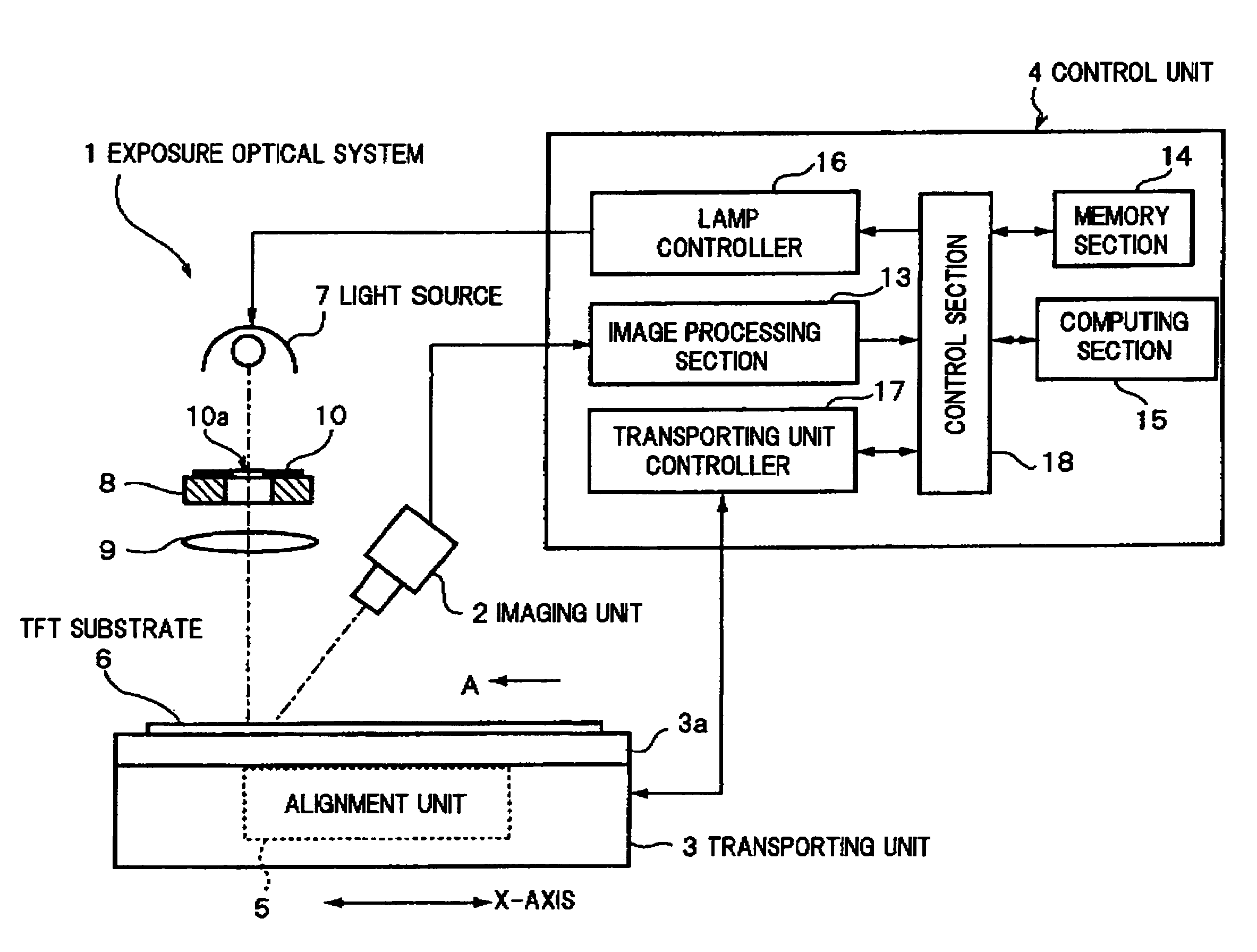
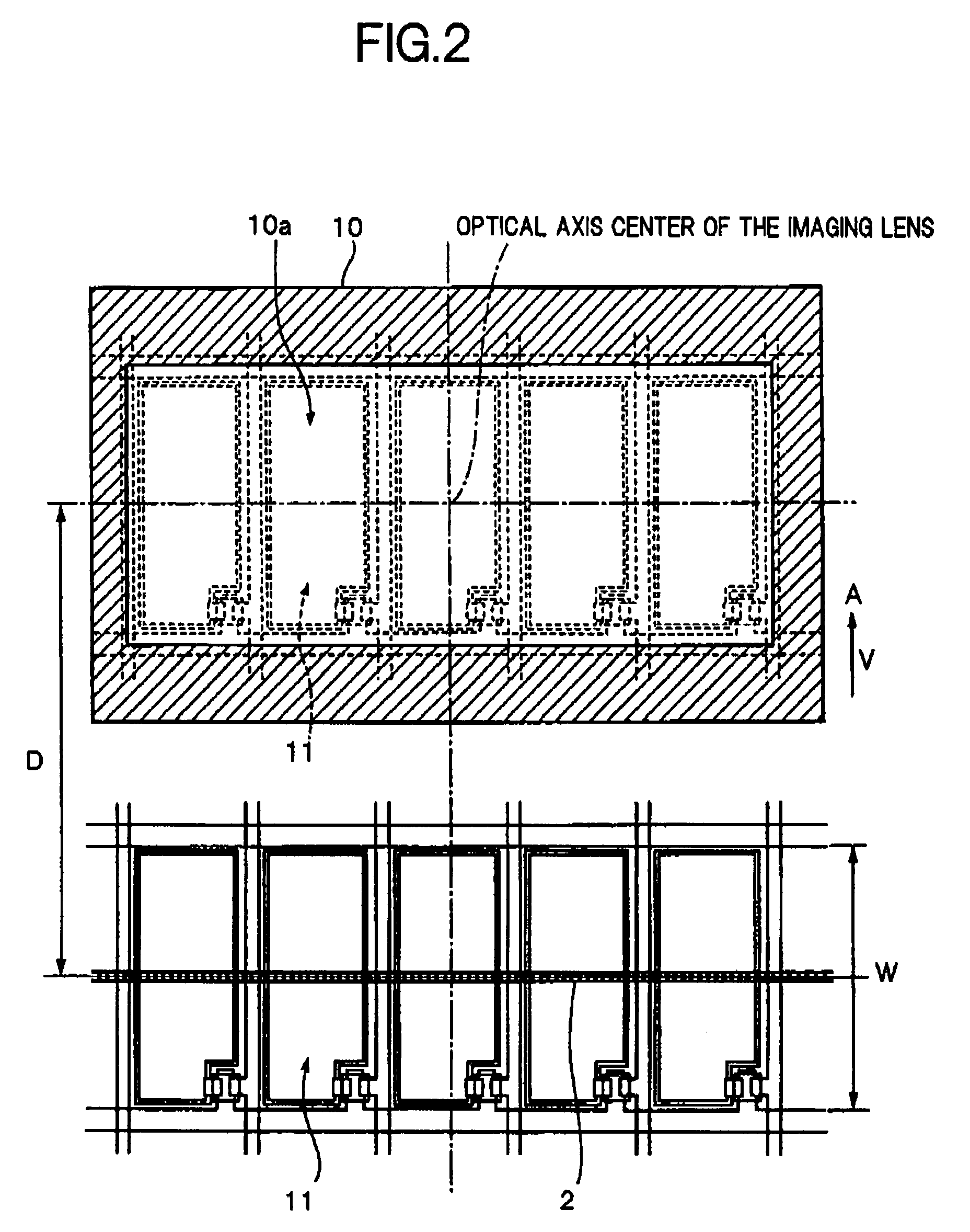
[0034]FIG. 1 is a conceptual block diagram showing a configuration of an exposure apparatus to be used for performing a production method of a substrate for a liquid crystal display according to the present invention. This exposure apparatus, irradiates exposure light with an exposure optical system, to expose a pattern of a color filter or a black matrix mask interposed on a path of the exposure optical system, onto a TFT substrate, and is provided with the exposure optical system 1, an imaging unit 2, a transporting unit 3, and a control unit 4.

[0035]The exposure optical system 1 irradiates exposure light on a TFT substrate 6 onto which a photosensitive colored resist (photosensitive material) of a color filter or a black matrix is applied by, e.g., coating, to expose a predetermined color filter or a black matrix pattern, and it is provided with a light sour...


PUM

PropertyMeasurementUnit
photosensitiveaaaaaaaaaa
velocityaaaaaaaaaa
period of timeaaaaaaaaaa

Abstract

A production method of a substrate for a liquid crystal display in which an exposure pattern of a color filter or a black matrix is formed in a predetermined position of a TFT substrate at a high level of precision. Therefore the production method includes following steps: applying a photosensitive material for a color filter or a black matrix onto a TFT substrate; image-capturing a pixel region by an imaging unit while transporting the TFT substrate coated with the photosensitive material at a predetermined velocity by a transporting unit; detecting a reference position preset in the pixel region image-captured by the imaging unit at an image processing section of a control unit; and controlling irradiation timing of a light source in an exposure optical system by a lamp controller with reference to the detected reference position, and forming an exposure pattern of a color filter or a black matrix at a predetermined position of the TFT substrate.

Description

[0001]This application is a continuation of PCT / JP2005 / 019894, filed on Oct. 28, 2005.BACKGROUND OF THE INVENTION[0002]1. Field of the Invention[0003]The present invention relates to a production method of a substrate for a liquid crystal display in which a color filter or a black matrix is directly formed on a TFT substrate on which a thin film transistor is formed for each pixel region, and in particular, relates to a production method of a substrate for a liquid crystal display in which a predetermined exposure pattern is formed in a predetermined position of the TFT substrate at a high level of precision, by detecting a reference position preset in a pixel region that has been image-captured while the TFT substrate was carried at a predetermined velocity, and controlling irradiation timing of exposure light.[0004]2. Description of the Related Art[0005]In general, a liquid crystal display has a configuration such that a liquid crystal is sealedly arranged between a pair of transp...

Claims


Application Information

Patent Timeline
Patent Type & Authority Patents(United States)
IPC IPC(8): G02F1/13G01B11/00
CPCG02F1/133516G02F1/136209G03F7/70525G03F7/70791G02F2001/136222G02F1/136222G02F1/13G02F1/1335
Inventor IINO, JIN
Owner V TECH CO LTD
Why Eureka
Try Eureka