Method and system for topography-aware reticle enhancement

a topography-aware, reticle technology, applied in the direction of semiconductor/solid-state device testing/measurement, instruments, photomechanical equipment, etc., can solve the problems of unreliable patterning accuracy, method and system cited above, affecting patterning accuracy and manufacturing yield, etc., to improve the design of the photomask, improve the performance of the integrated circuit, and reduce the error in the transfer of an ic layou

Inactive Publication Date: 2010-10-12
RPX CORP
View PDF8 Cites 19 Cited by
  • Summary
  • Abstract
  • Description
  • Claims
  • Application Information

AI Technical Summary

Benefits of technology

[0013]Another object of the invention is to reduce the critical dimension error induced by a non-planar topography of a wafer layer.
[0016]Yet another object of the invention is to increase parametric yield in manufactured ICs.
[0018]The incorporation of predicted topographic variations underlying a given wafer layer of the IC during RET calculations improves the design of the photomask(s) for the given wafer layer. In other words, the predicted topographic variation leads to predicted defocus values, and by assigning individual features of the IC layout to specific DMLs, the OPC, SRAF or other RET calculations of the photomask layout become more accurate. This considerably reduces the errors in transfer of an IC layout onto a wafer layer. The topographic variations are incorporated taking into account design objectives, such timing delay and power, thereby improving the performance of the integrated circuit. Further, the method increases the parametric yield in the manufactured IC.

Problems solved by technology

These changes are due to various manufacturing non-idealities, including optical effects such as scattering of light, as well as focus variations (i.e., variations in the distance between a lens and the wafer layer).
However, with advanced lithographic processes and small feature dimensions, imperfect planarity—i.e., topographic variation—of wafer layers has become a major cause of focus variation in the succeeding layers to be manufactured.
The methods and systems cited above do not take into account systematic and predictable post-planarization topographic variations of the wafer surface.
Yet, such wafer topographic variations affect focus in a lithography process which in turn affects patterning accuracy and manufacturing yield—both functional and parametric—of the IC.

Method used


Image

  • Method and system for topography-aware reticle enhancement
  • Method and system for topography-aware reticle enhancement
  • Method and system for topography-aware reticle enhancement

Examples


Embodiment Construction

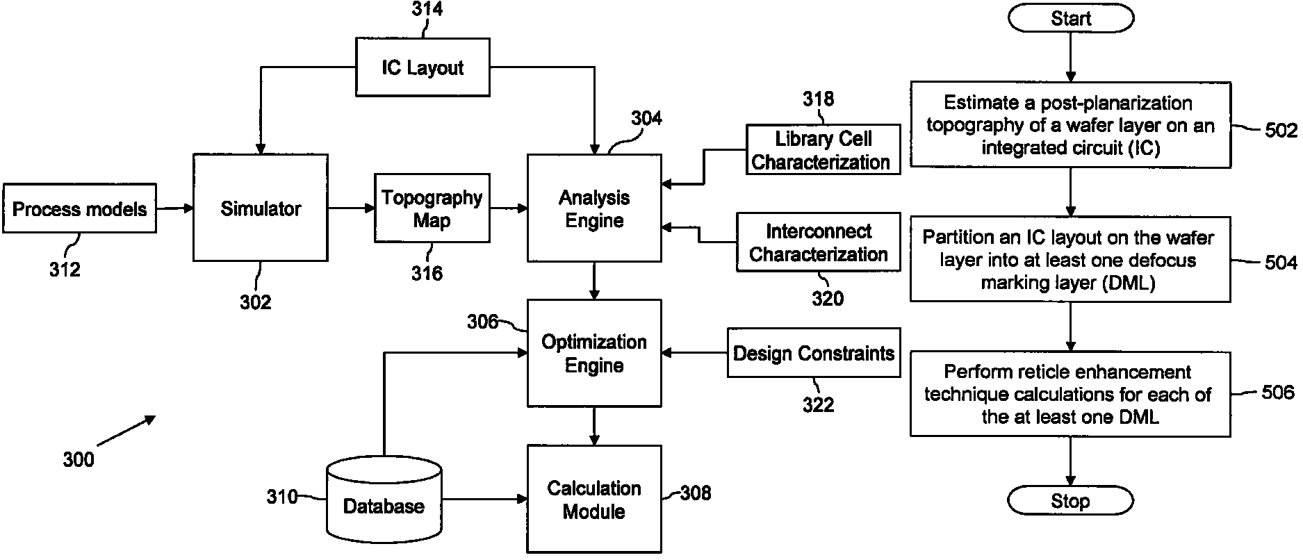
[0029]Various embodiments of the present invention provide a method, system, and a computer program product for reticle enhancement during manufacture of an integrated circuit (IC). A post-planarization topography of a wafer layer on the IC is estimated. Reticle enhancement technique calculations (RET) such as optical proximity correction and phase-shifting are performed taking into consideration the post-planarization topography of the wafer layer, thereby increasing the parametric yield in the manufactured IC.

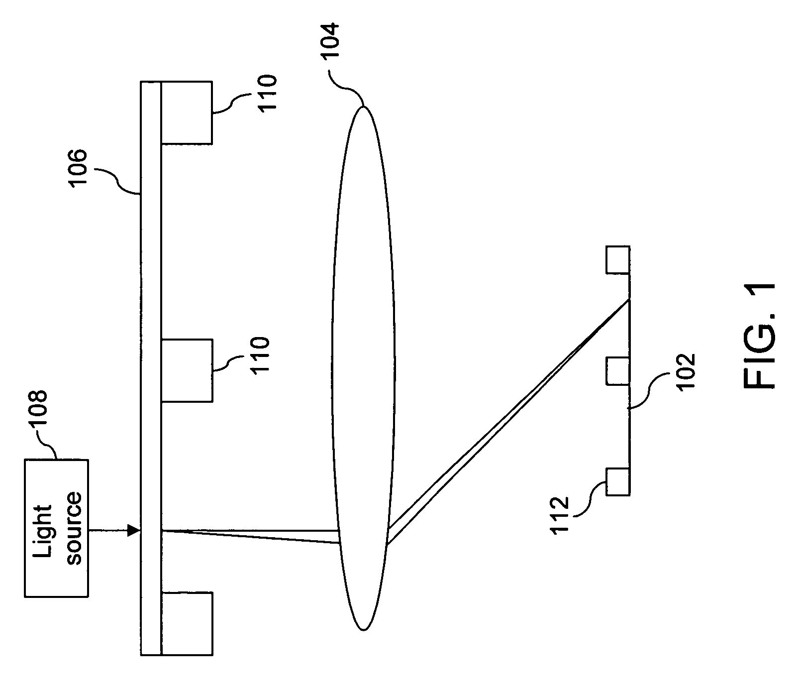
[0030]FIG. 1 is a block diagram illustrating an optical lithographic system 100, in accordance with an embodiment of the invention. Optical lithographic system 100 creates a reduced circuit pattern image on a wafer layer 102 during lithography. Optical lithographic system 100 includes a lens 104, a reticle 106, and a light source 108.

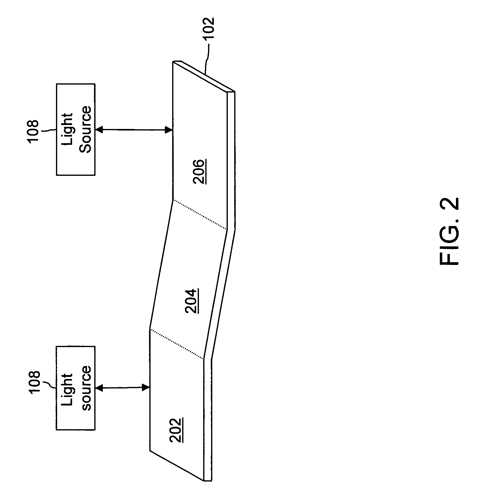
[0031]Wafer layer 102 is a semiconductor layer on which an IC layout is to be created. The IC layout represents patterns of IC devices to be pri...


PUM


Abstract

The present invention provides a method and system for improving reticle enhancement calculations during manufacture of an integrated circuit (IC). The reticle enhancement calculations are improved by incorporating post-planarization topography estimates. A planarization process of a wafer layer is simulated to estimate the post-planarization topography. RET calculations, such as sub-resolution assist feature insertion, optical proximity corrections and phase shifting are then performed based on the post-planarization topography of the wafer layer.

Description

[0001]This application claims priority to Provisional Application 60 / 630,072, filed Nov. 22, 2004, entitled System and Method for Topography-Aware Reticle Enhancement.BACKGROUND OF THE INVENTION[0002]1. Field of the Invention[0003]The present invention relates to the field of semiconductor circuits and, in particular, to a method and system for improving the manufacturing process of an integrated circuit (IC).[0004]2. Description of the Related Art[0005]In an IC fabrication process, optical lithography using one or more photomasks is applied to transfer designed circuit patterns onto a given wafer layer (e.g., active area, transistor gate polysilicon, contact, Metal-1, etc.) of an integrated circuit (IC). These circuit patterns represent layout features of the IC. Over the past few years, the dimensions of the layout features in ICs have been reduced to achieve greater circuit operating frequencies and increased integration densities. With reduced dimensions, advanced photomasks hav...

Claims


Application Information

Patent Timeline
Patent Type & Authority Patents(United States)
IPC IPC(8): G06F17/50
CPCG03F1/144G03F1/36G03F7/70433G03F7/70441G03F7/705G03F7/70783H01L22/20H01L2924/0002H01L2924/00G03F1/70
Inventor GUPTA, PUNEETKAHNG, ANDREW B.
Owner RPX CORP
Why Eureka
Try Eureka