Power supply voltage converting circuit, method for controlling the same, display device, and mobile terminal

a power supply voltage and conversion circuit technology, applied in the direction of dc-dc conversion, static indicating devices, instruments, etc., can solve the problems of large circuit size, difficult to control the voltage of the power supply, and the miniaturization of the display, so as to reduce the transistor size increase the voltage between the gate and the source of the transistor pair, and increase the voltage of the transistor pair.

Active Publication Date: 2010-10-26
JAPAN DISPLAY WEST
View PDF28 Cites 1 Cited by
  • Summary
  • Abstract
  • Description
  • Claims
  • Application Information

AI Technical Summary

Benefits of technology

[0008]In the supply voltage conversion circuit with the above-described configuration, amplitude conversion is implemented to convert from the control pulse with amplitude corresponding to the first supply voltage to the control pulse with amplitude corresponding to the second supply voltage. The control pulse having the converted amplitude is then applied to the pair of transistors for charging / discharging the capacitor. Thus, the voltages between the gate and source of the pair of transistors are increased. Accordingly, the on-resistance of the transistor pair is decreased, and therefore the transistor sizes of the transistor pair can be decreased. As a result, a supply voltage conversion circuit having a large current capability can be achieved with a small circuit scale.

Problems solved by technology

Therefore, when realization of a DC-DC converter of large current capacitance is aimed, large size transistors need to be formed, which leads to a large circuit size.
This circuit size increase is problematically significant when the circuits are fabricated using devices having comparatively small mobility such as low-temperature poly-silicon TFT (Thin Film Transistor), which are formed on an insulating substrate.
Therefore, a serious problem arises when miniaturization of a display is aimed.

Method used


Image

  • Power supply voltage converting circuit, method for controlling the same, display device, and mobile terminal
  • Power supply voltage converting circuit, method for controlling the same, display device, and mobile terminal
  • Power supply voltage converting circuit, method for controlling the same, display device, and mobile terminal

Examples


first embodiment

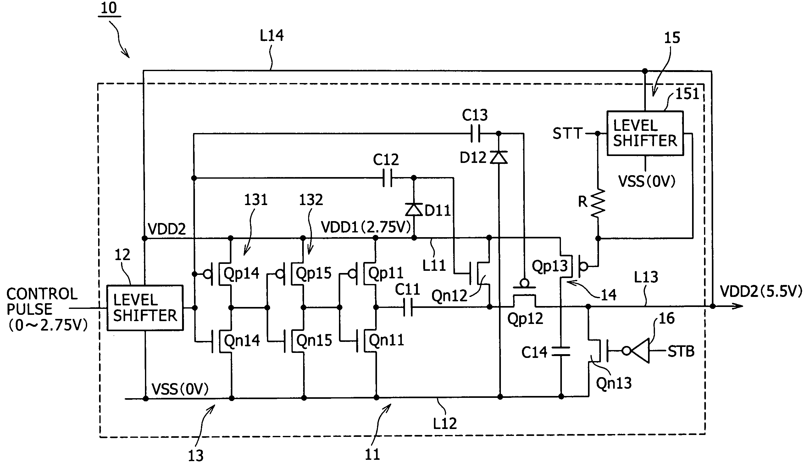
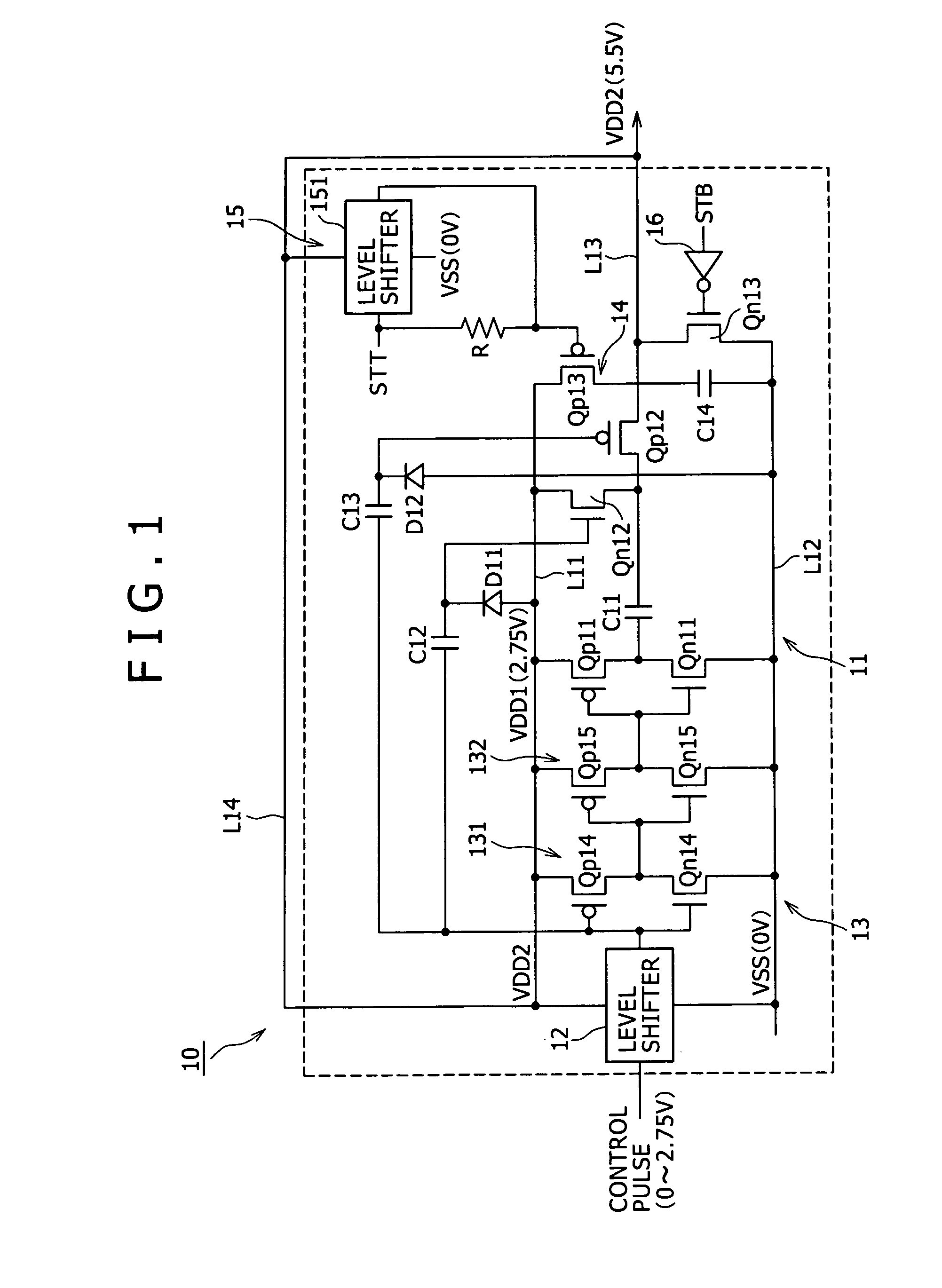
[0019]FIG. 1 is a circuit diagram illustrating an example of the configuration of a DC voltage conversion circuit, i.e., a charge pump DC-DC converter, according to a first embodiment of the present invention. Here, as one example, description will be made about a DC-DC converter supplied with a first positive supply voltage VDD1 of 2.75 V and a negative supply voltage VSS of 0 V (ground level), and boosting the first positive supply voltage VDD1 to twice the voltage VDD1, i.e., to a second positive supply voltage VDD2 of 5.5 V.

[0020]As is apparent from FIG. 1, a DC-DC converter 10 according to the present embodiment includes a charge pump circuit 11, a level shifter 12, a buffer 13, a switch element 14 and a power supply start-up control circuit 15. The charge pump circuit 11 includes a flying capacitor C11 and a pair of transistors for charging / discharging the flying capacitor C11, i.e., a PchMOS transistor Qp11 and an NchMOS transistor Qn11. The PchMOS transistor Qp11 is connecte...

second embodiment

[0040]FIG. 4 is a circuit diagram illustrating an example of the configuration of a DC voltage conversion circuit, i.e., a charge pump DC-DC converter, according to a second embodiment of the present invention. Here, as one example, description will be made about a DC-DC converter supplied with a first positive supply voltage VDD1 of 2.75 V and a first negative supply voltage VSS1 of 0 V (ground level), and boosting the first positive supply voltage VDD1 to a second positive supply voltage VDD2 of 5.5 V (boosting to twice the voltage VDD1) and converting the voltage VDD1 to a second negative supply voltage VSS2 of −2.75 V (converting by a factor of minus one).

[0041]As is apparent from FIG. 4, a DC-DC converter 20 according to the present embodiment is composed of three blocks: control circuit unit 21, 5.5 V generation circuit unit 22, and −2.75 V generation circuit unit 23. The control circuit unit 21 employs the positive supply voltage VDD1, which is the logic level voltage, and th...

application example

[0076]Charge pump DC-DC converters (supply voltage conversion circuits) according to the above-described embodiments are used as, e.g., a power supply circuit of a flat-panel display typified by liquid crystal displays in which pixels that employ liquid crystal cells as electro-optical elements are two-dimensionally arranged in rows and columns. FIG. 7 illustrates one example of the configuration thereof. Here, description will be made by taking as an example an active matrix liquid crystal display.

[0077]Referring to FIG. 7, mounted on a transparent insulating substrate, e.g., a glass substrate 31 are a display area part 32 in which a number of pixels including liquid crystal cells are two-dimensionally arranged in rows and columns, a pair of upside and downside H drivers (horizontal drive circuits) 33U and 33D, a V driver (vertical drive circuit) 34, and a supply voltage conversion circuit 35. As the supply voltage conversion circuit 35, a charge pump DC-DC converter according to a...


PUM


Abstract

A supply voltage conversion circuit allowing fabrication of a charge pump circuit having a large current capability with a small area is provided. In a charge pump DC-DC converter (10) for converting a supply voltage VDD1 to a supply voltage VDD2, a level shifter (12) implements amplitude conversion to convert from a control pulse with amplitude of VSS-VDD1 to a control pulse with amplitude of VSS-VDD2. By using the control pulse having the converted amplitude as a pumping pulse, a flying capacitor (C11) is charged / discharged by MOS transistors (Qp11), and (Qn11) of a charge pump circuit (11), and switching of MOS transistors (Qn12), and (Qp12) coupled to the output of the flying capacitor (C11) is controlled.

Description

TECHNICAL FIELD[0001]The present invention relates to a supply voltage conversion circuit, a control method thereof, a display and a portable terminal, and particularly to a supply voltage conversion circuit employing a charge pump circuit that charges / discharges a capacitor, a control method thereof, a display having the supply voltage conversion circuit, and a portable terminal typified by a cellular phone employing the display as its screen display part.BACKGROUND ART[0002]In recent years, spread of portable terminals, such as cellular phones and PDAs (Personal Digital Assistants; portable information terminals), have been remarkable. One factor of the rapid spread of these portable terminals is, for example, liquid crystal displays included as a screen display part of the portable terminals. The reason for this is that the liquid crystal displays are display devices that have a characteristic of requiring no power for driving themselves in principle, and therefore are of low pow...

Claims


Application Information

Patent Timeline
Patent Type & Authority Patents(United States)
IPC IPC(8): G09G5/00H02M3/07
CPCH02M3/073H02M2003/076H02M3/076H02M3/07
Inventor NAKAJIMA, YOSHIHARUKIDA, YOSHITOSHI
Owner JAPAN DISPLAY WEST
Why Eureka
Try Eureka