Nonvolatile semiconductor memory circuit utilizing a MIS transistor as a memory cell

a technology of mis transistor and memory cell, which is applied in the field of memory circuits, can solve problems such as circuits that do not function properly as designed, and achieve the effect of reducing the threshold voltage of the mis transistor and relatively low resistance of the highly doped substrate layer

Active Publication Date: 2010-10-26
NSCORE
View PDF20 Cites 65 Cited by
  • Summary
  • Abstract
  • Description
  • Claims
  • Application Information

AI Technical Summary

Benefits of technology

[0011]It is a general object of the present invention to provide a memory circuit that substantially eliminates one or more problems caused by the limitations and disadvantages of the related art.
[0012]It is another and more specific object of at least one embodiment of the present invention to provide a memory circuit that can suppress an adverse effect caused by impact ionization.
[0016]According to at least one embodiment, the resistance of the highly-doped substrate layer is relatively low in comparison with the resistance of an ordinary substrate, so that a potential difference existing between the source of the MIS transistor and an externally applied substrate potential is suppressed. A reduction in the threshold voltage of the MIS transistor is thus decreased.

Problems solved by technology

There is thus a risk that the circuit does not function properly as designed.

Method used


Image

  • Nonvolatile semiconductor memory circuit utilizing a MIS transistor as a memory cell
  • Nonvolatile semiconductor memory circuit utilizing a MIS transistor as a memory cell
  • Nonvolatile semiconductor memory circuit utilizing a MIS transistor as a memory cell

Examples


Embodiment Construction

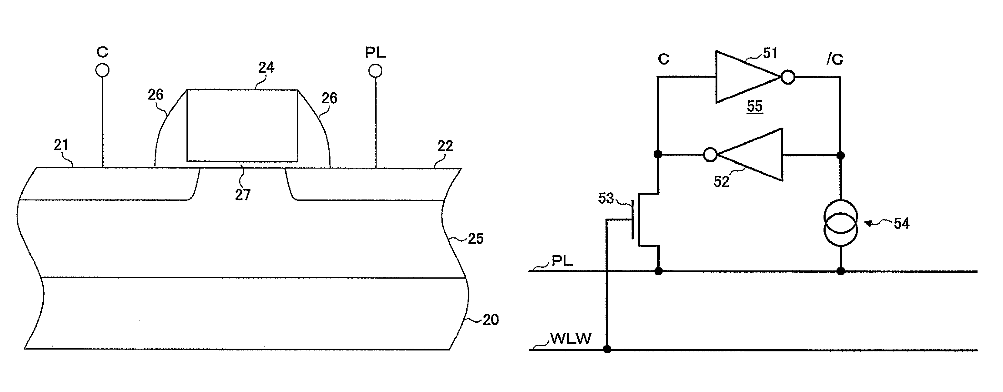
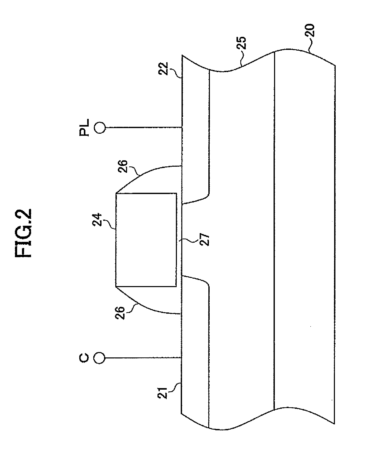
[0028]The present invention is directed to PermSRAM. Namely, the memory cell transistors are MIS (metal-insulating film-semiconductor) transistors that have the same structure as ordinary MIS transistors used for conventional transistor functions (e.g., switching function). These memory cell transistors use neither a special structure such as a floating gate nor a special material such as a ferroelectric material or a ferromagnetic material. These MIS transistors are configured to selectively experience a hot-carrier effect on purpose for storage of one-bit data. The hot-carrier effect leaves an irreversible lingering change in the transistor characteristics to the MIS transistors. A change in the transistor characteristics caused by the hot-carrier effect achieves nonvolatile data retention.

[0029]In the following description, NMOS transistors are used as an example of the nonvolatile-memory-cell MIS transistors, but such examples are not intended to be limiting. PMOS transistors ma...


PUM


Abstract

A memory circuit includes a latch having a first node and a second node to store data such that a logic level of the first node is an inverse of a logic level of the second node, a MIS transistor having a gate node, a first source / drain node, and a second source / drain node, the first source / drain node coupled to the first node of the latch, and a control circuit configured to control the gate node and second source / drain node of the MIS transistor in a first operation such that a lingering change is created in transistor characteristics of the MIS transistor in response to the data stored in the latch, wherein the MIS transistor includes a highly-doped substrate layer, a lightly-doped substrate layer disposed on the highly-doped substrate layer, diffusion regions formed in the lightly-doped substrate layer, a gate electrode, sidewalls, and an insulating film.

Description

BACKGROUND OF THE INVENTION[0001]1. Field of the Invention[0002]The disclosures herein generally relate to a memory circuit, and particularly relate to a nonvolatile memory circuit which is capable of retaining stored data in the absence of a power supply voltage.[0003]2. Description of the Related Art[0004]Nonvolatile semiconductor memory devices, which can retain stored data even when power is turned off, conventionally include flash EEPROM employing a floating gate structure, FeRAM employing a ferroelectric film, MRAMs employing a ferromagnetic film, etc. There is a new type of nonvolatile semiconductor memory device called PermSRAM. PermSRAM uses a MIS (metal-insulating film-semiconductor) transistor as a nonvolatile memory cell (i.e., the basic unit of data storage). The MIS transistor used as a nonvolatile memory cell in PermSRAM has the same structure as ordinary MIS transistors used for conventional transistor functions (e.g., switching function), and do not require a specia...

Claims


Application Information

Patent Timeline
Patent Type & Authority Patents(United States)
IPC IPC(8): G11C17/12
CPCG11C11/412G11C14/00H01L21/28282H01L27/11565H01L29/792H01L29/40117H10B43/10
Inventor HORIUCHI, TADAHIKO
Owner NSCORE
Why Eureka
Try Eureka