Method of forming through-silicon vias

a technology of silicon vias and through-silicon vias, which is applied in the direction of semiconductor devices, semiconductor/solid-state device details, electrical apparatus, etc., can solve the problems of minimum size needed to make these components, physical limits of the density that can be achieved in two dimensions, and the requirement of more complex designs

Active Publication Date: 2010-11-02
TAIWAN SEMICON MFG CO LTD
View PDF6 Cites 161 Cited by
  • Summary
  • Abstract
  • Description
  • Claims
  • Application Information

AI Technical Summary

Benefits of technology

[0008]These and other problems are generally solved or circumvented, and technical advantages are generally achieved, by embodiments of the present invention which provide for a semiconductor device having a through-silicon via (TSV).

Problems solved by technology

Although dramatic improvement in lithography has resulted in considerable improvement in 2D integrated circuit formation, there are physical limits to the density that can be achieved in two dimensions.
One of these limits is the minimum size needed to make these components.
Also, when more devices are put into one chip, more complex designs are required.
Furthermore, due to the topography of the wafer, a copper residue may remain over the surface of the wafer.

Method used


Image

  • Method of forming through-silicon vias
  • Method of forming through-silicon vias
  • Method of forming through-silicon vias

Examples


Embodiment Construction

[0016]The making and using of the present embodiments are discussed in detail below. It should be appreciated, however, that the present invention provides many applicable inventive concepts that can be embodied in a wide variety of specific contexts. The specific embodiments discussed are merely illustrative of specific ways to make and use the invention, and do not limit the scope of the invention.

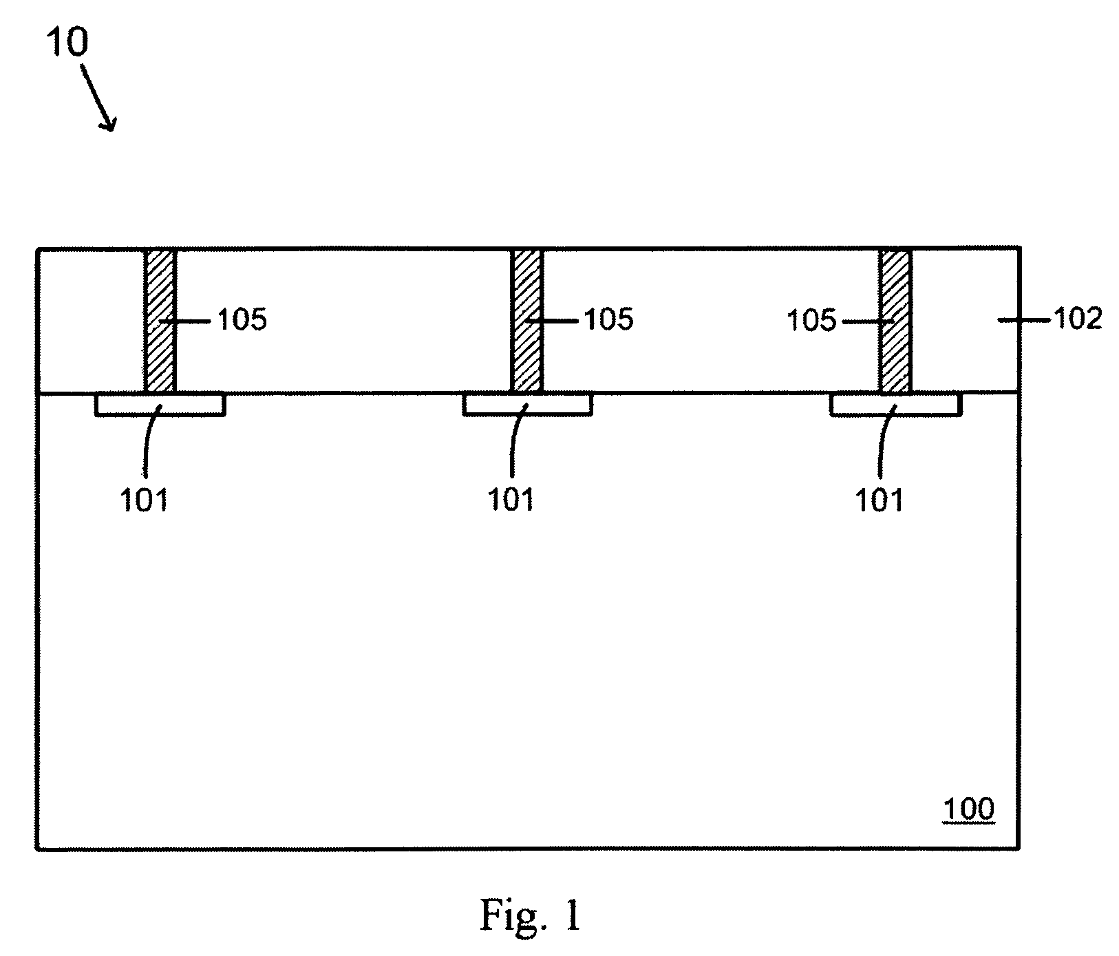
[0017]With reference now to FIG. 1, there is shown a cross-sectional diagram of wafer 10. Wafer 10 comprises semiconductor substrate 100, which is typically silicon (Si), but may also be made of gallium arsenide (GaAs), gallium arsenide-phosphide (GaAsP), indium phosphide (InP), gallium aluminum arsenic (GaAlAs), indium gallium phosphide (InGaP), and the like, and illustrates devices 101 formed in the substrate 100. While only three devices 101 are shown, there may be many active and passive semiconductor devices 101 formed in substrate 100.

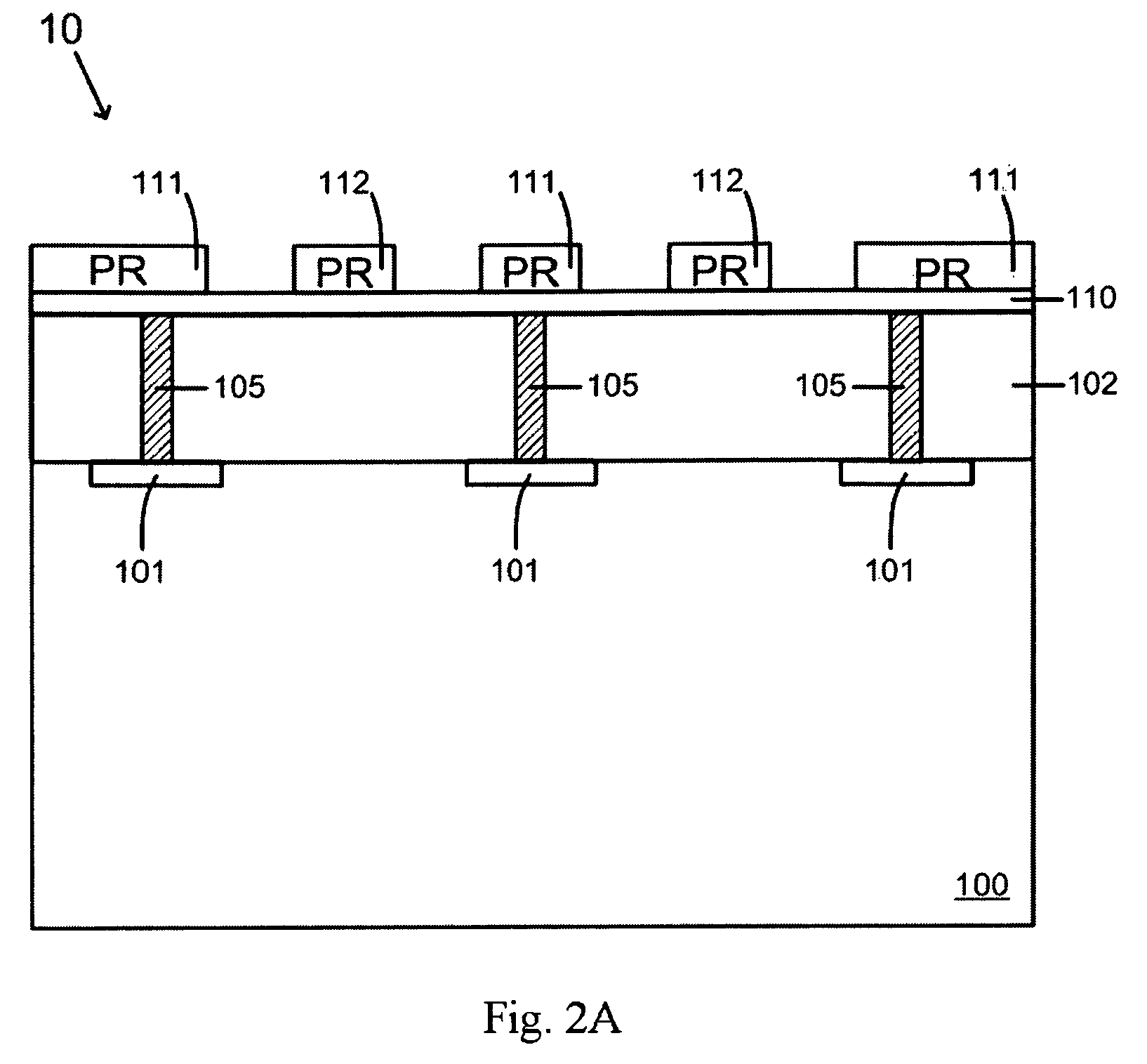
[0018]Insulating layer (also sometimes referred...


PUM

PropertyMeasurementUnit
thicknessaaaaaaaaaa
depthaaaaaaaaaa
stacking structureaaaaaaaaaa

Abstract

A method of forming a semiconductor device having a through-silicon via (TSV) is provided. A semiconductor device is provided having a first dielectric layer formed thereon. One or more dielectric layers are formed over the first dielectric layer, such that each of the dielectric layers have a stacking structure, wherein the stacking structures in the one or more dielectric layers are vertically aligned. The stacking structures may be, for example, metal rings. The stacking structures are then removed to form a first recess. A second recess is formed by extending the first recess into the substrate. The second recess is filled with a conductive material to form the TSV.

Description

TECHNICAL FIELD[0001]The present invention relates generally to integrated circuit fabrication and, more particularly, to a method of forming through-silicon vias in a semiconductor die and the resulting stacked dice structure.BACKGROUND[0002]Since the invention of the integrated circuit (IC), the semiconductor industry has experienced continued rapid growth due to continuous improvements in the integration density of various electronic components (e.g., transistors, diodes, resistors, capacitors, etc.). For the most part, this improvement in integration density has come from repeated reductions in minimum feature size, which allows more components to be integrated into a given area.[0003]These integration improvements are essentially two-dimensional (2D) in nature, in that the volume occupied by the integrated components is essentially on the surface of the semiconductor wafer. Although dramatic improvement in lithography has resulted in considerable improvement in 2D integrated ci...

Claims


Application Information

Patent Timeline
Patent Type & Authority Patents(United States)
IPC IPC(8): H01L21/4763
CPCH01L21/76898H01L25/0657H01L25/50H01L2225/06513H01L2225/06541H01L2224/16H01L24/03H01L24/05H01L2224/0401H01L2224/05001H01L2224/05009H01L2224/05124H01L2224/05139H01L2224/05144H01L2224/05147H01L2224/05184H01L2224/05568H01L2224/05609H01L2224/05616H01L2224/05624H01L2224/05644H01L2224/05647H01L2224/05684H01L2924/00014H01L2924/0105H01L2924/01079H01L2924/013H01L2924/01029
Inventor LIN, CHUAN-YILEE, SONG-BORHUANG, CHING-KUNLIN, SHENG-YUAN
Owner TAIWAN SEMICON MFG CO LTD
Why Eureka
Try Eureka