
Thermosetting die-bonding film

a technology of die-bonding film and die-bonding film, which is applied in the direction of transportation and packaging, synthetic resin layered products, chemistry apparatus and processes, etc., can solve the problems of poor reliability of bonding a semiconductor chip, low bonding strength between the electrode member and the semiconductor chip, and poor characteristic, so as to prevent the generation of voids and reduce the number of pickup steps. , the effect of high reliability

Inactive Publication Date: 2010-11-09
NITTO DENKO CORP
View PDF7 Cites 5 Cited by
  • Summary
  • Abstract
  • Description
  • Claims
  • Application Information

AI Technical Summary

Benefits of technology

[0021]The present invention has an effect described below by the means explained above.
[0022]That is, according to the present invention, by containing 15 to 30% by weight of a thermoplastic resin component and 60 to 70% by weight of a thermosetting resin component as main components and setting a surface free energy before heat curing to 37 mJ / m2 or more and less than 40 mJ / m2, adhesion to the adherent is improved and the generation of voids in prevented, and the pickup properties during the pickup step are made to be preferable. As a result, it becomes possible to manufacture a semiconductor device having high reliability with preferable yield.

Problems solved by technology

As a result, the thickness of the formed paste-form adhesive layer becomes uneven so that the reliability in strength of bonding a semiconductor chip is poor.
In other words, if the amount of the paste-form adhesive coated on an electrode member is insufficient, the bonding strength between the electrode member and a semiconductor chip becomes low so that in a subsequent wire bonding step, the semiconductor chip is peeled.
On the other hand, if the amount of the coated paste-form adhesive is too large, this adhesive flows out to stretch over the semiconductor chip so that the characteristic becomes poor.
Thus, the yield or the reliability lowers.
Such problems about the adhesion treatment become particularly remarkable with an increase in the size of semiconductor chips.
Thus, the workability or the productivity is deteriorated.
In this method, however, it is difficult to make the paste-form adhesive layer even.
Moreover, an especial machine or a long time is required to coat the paste-form adhesive.
However, if the melt viscosity is too low, an adhesive bleeds out from the adhesive film to result in a problem that the adhesive pollutes the substrate or the semiconductor chip.
On the other hand, if the melt viscosity is too high, the adhesiveness of the film onto an adherend deteriorates to result in a problem that voids are generated.
There is often a case that the die-bonding film of a dicing die-bonding film of this type is formed on the entire surface of an adhesive layer (an adhesive film) due to limitation of its manufacturing step.
However, in such case, there has been a case that the dicing ring is contaminated because the dicing ring is adhered to the die-bonding film.
However, in such a case, there is a case that air bubbles (voids) are generated between the die-bonding film and the chip and between the die-bonding film and the adherent during die bonding.
As a result, it becomes a cause of generating troubles in a produced semiconductor device.
However, because the surface free energy is high, the adhesion with the dicing film is improved, and thus, the die-bonding film and the dicing film cannot be peeled in the pickup step, and there is a problem that the pickup cannot be performed.

Method used

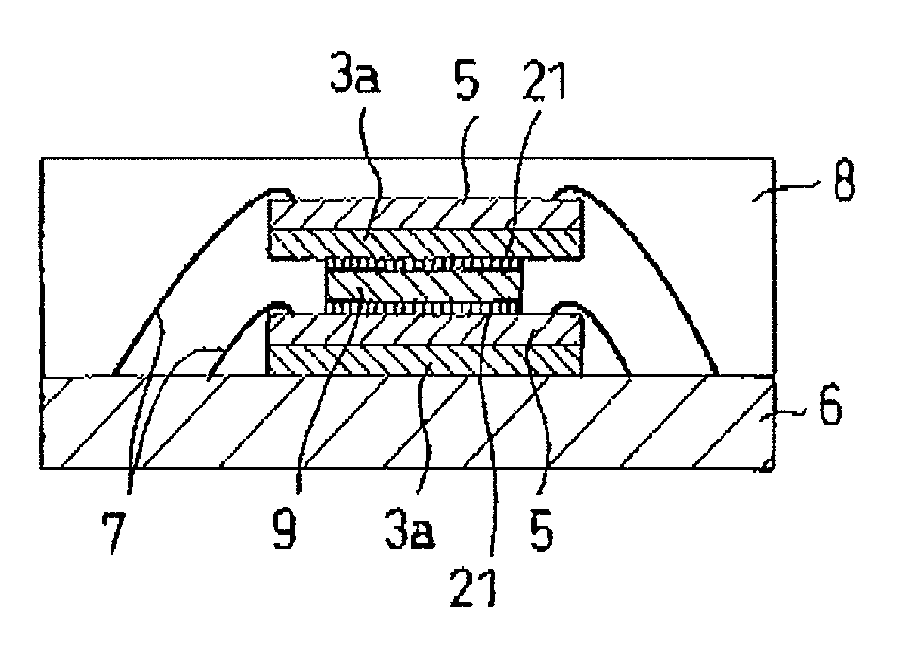
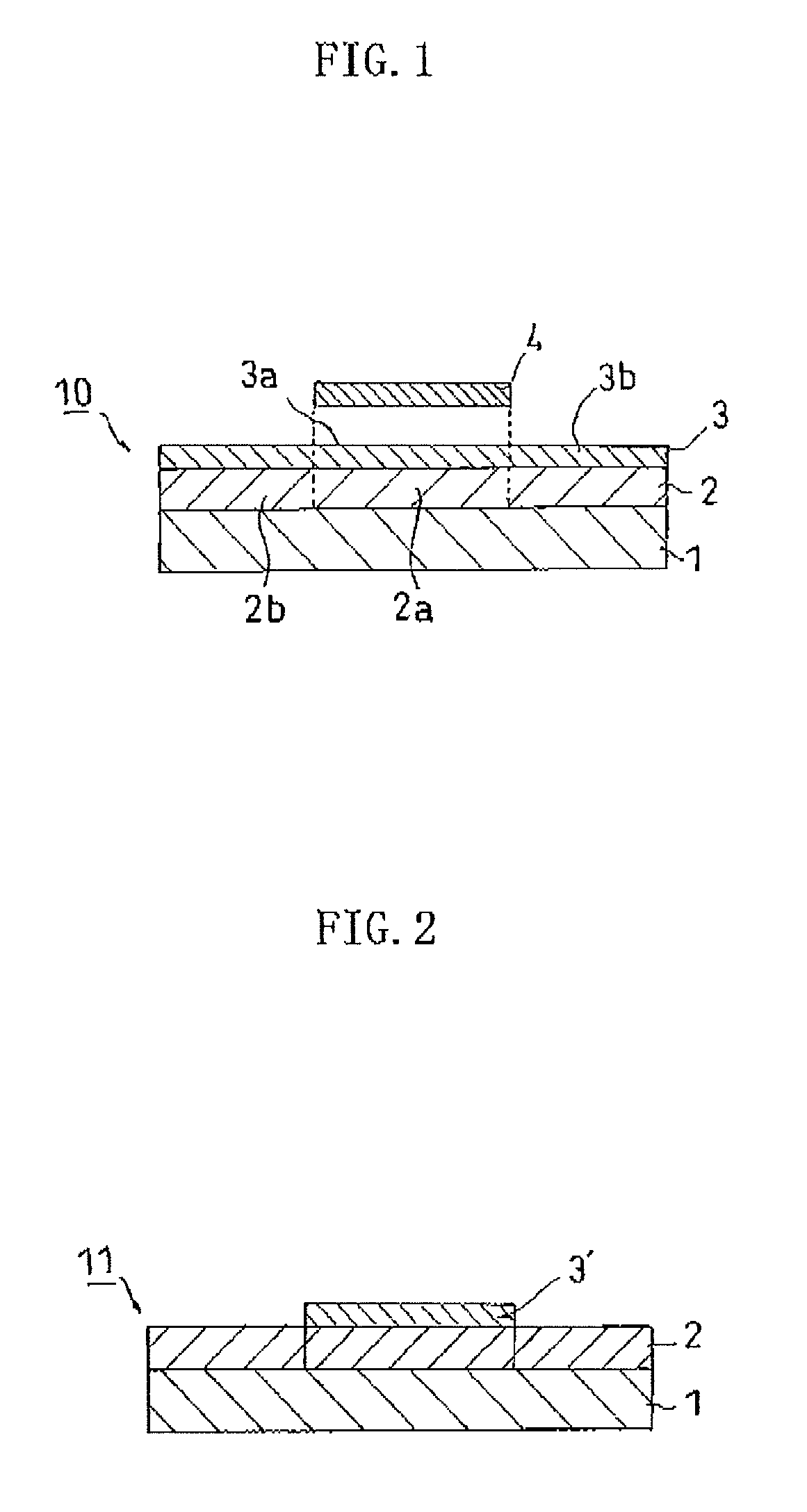
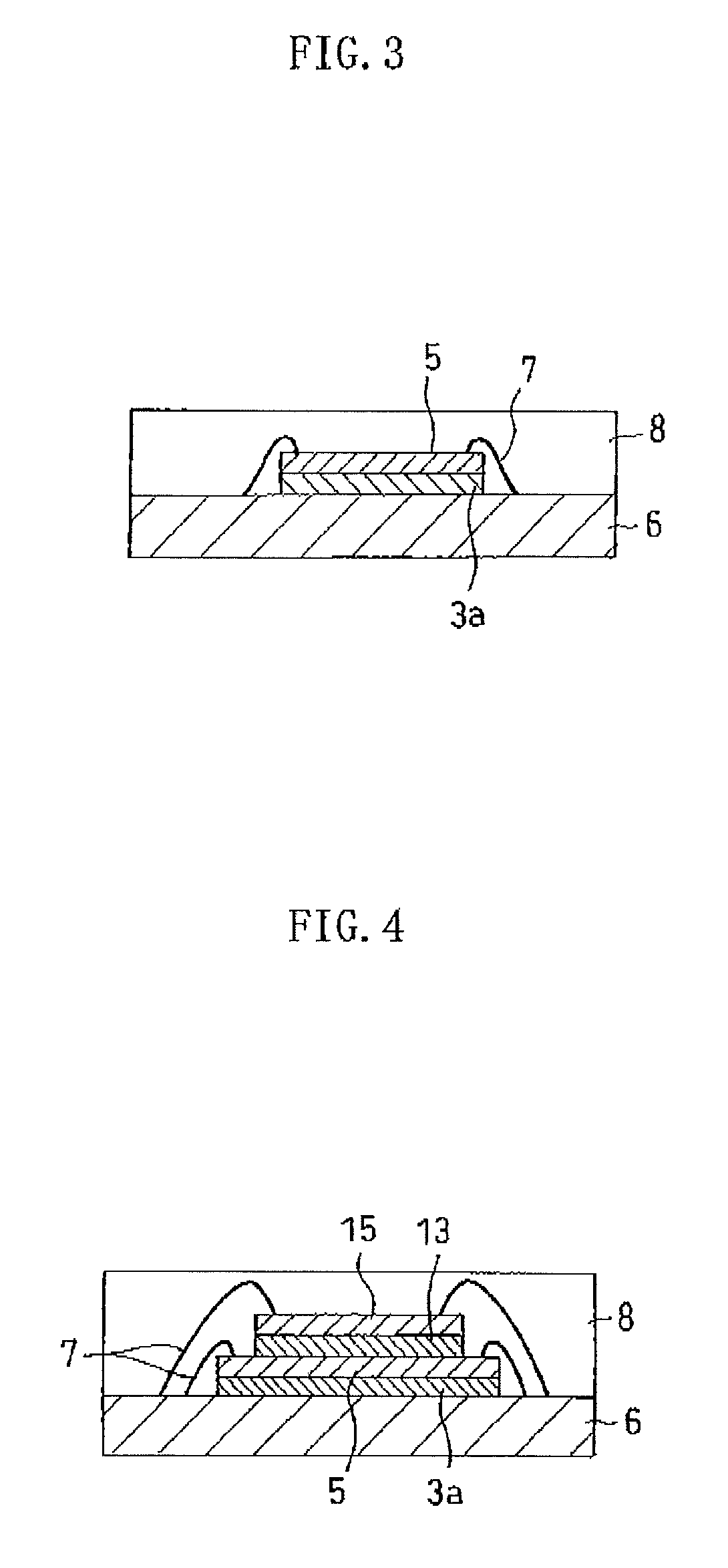

Image

  • Thermosetting die-bonding film
  • Thermosetting die-bonding film
  • Thermosetting die-bonding film

Examples


example 1

[0112]An adhesive composition having a concentration of 23.6% by weight was prepared by dissolving 144 parts of an epoxy resin 1 (EPIKOTE 1004 manufactured by Japan Epoxy Resins Co., Ltd.), 130 parts of an epoxy resin 2 (EPIKOTE 827 manufactured by Japan Epoxy Resins Co., Ltd.), 293 parts of a phenol resin (MILEX XLC-4L manufactured by Mitsui Chemicals, Inc.), 444 parts of sphere-shaped silica (SO-25R manufactured by Admax Co., Ltd.) and 2 parts of a curing catalyst (C11-Z manufactured by Shikoku Chemicals Corporation) based on 100 parts by weight of an acrylic ester polymer (Parakuron W-197CM manufactured by Negami Chemical Industrial Co., Ltd.) containing ethyl acrylate-methylmethacrylate as a main component into methylethylketone.

[0113]This solution of the adhesive composition was applied onto a release treated film made of a polyethylene terephthalate film having a thickness of 50 μm on which a silicone releasing treatment was performed as a releasing liner, and it was dried at ...

example 2

[0114]An adhesive composition having a concentration of 23.6% by weight was prepared by dissolving 126 parts of an epoxy resin 1 (EPIKOTE 1004 manufactured by Japan Epoxy Resins Co., Ltd.), 68 parts of an epoxy resin 2 (EPIKOTE 827 manufactured by Japan Epoxy Resins Co., Ltd.), 206 parts of a phenol resin (MILEX XLC-4L manufactured by Mitsui Chemicals, Inc.), 333 parts of sphere-shaped silica (SO-25R manufactured by Admax Co., Ltd.), and 1.5 parts of a curing catalyst (C11-Z manufactured by Shikoku Chemicals Corporation) based on 100 parts by weight of an acrylic ester polymer (Parakuron W-197CM manufactured by Negami Chemical Industrial Co., Ltd.) containing ethyl acrylate-methylmethacrylate as a main component into methylethylketone.

[0115]This solution of the adhesive composition was applied onto a release treated film made of a polyethylene terephthalate film having a thickness of 50 μm which a silicone releasing treatment was performed as a releasing liner, and it was dried at 1...


PUM

PropertyMeasurementUnit
surface free energyaaaaaaaaaa
tensile storage modulusaaaaaaaaaa

Abstract

A thermosetting die-bonding film having excellent adhesion to an adherent and preferable pickup properties and a dicing die-bonding film having the thermosetting die-bonding film are provided. The thermosetting die-bonding film of the present invention is a thermosetting die-bonding film that is used when manufacturing a semiconductor device and contains 15 to 30% by weight of a thermoplastic resin component and 60 to 70% by weight of a thermosetting resin component as main components, wherein a surface free energy before heat curing is 37 mJ / m2 or more and less than 40 mJ / m2.

Description

[0001]This application is the U.S. National Phase under 35 U.S.C. §371 of International Application No. PCT / JP2008 / 051772, filed Feb. 4, 2008, which claims priority to the Japanese Patent Application No. 2007-051767, filed Mar. 1, 2007. The International Application was not published in English under PCT Article 21(2).TECHNICAL FIELD[0002]The present invention relates to a thermosetting die-bonding film and a dicing die-bonding film having the thermosetting die-bonding film, and more specifically relates a thermosetting die-bonding film that is used when die bonding a semiconductor chip etc. onto an adherent such as a substrate and a lead frame, and a dicing die-bonding film having the thermosetting die-bonding film.BACKGROUND ART[0003]Conventionally, silver paste has been used to bond a semiconductor chip to a lead frame or an electrode member in the step of producing a semiconductor device. The treatment for the sticking is conducted by coating a paste-form adhesive on a die pad o...

Claims


Application Information

Patent Timeline
Patent Type & Authority Patents(United States)
IPC IPC(8): H01L21/00
CPCH01L21/6836H01L23/49513H01L23/49575H01L24/27H01L24/32H01L24/83H01L24/85H01L25/50H01L24/29H01L23/3121H01L24/45H01L2221/68327H01L2224/274H01L2224/2919H01L2224/32145H01L2224/32225H01L2224/45124H01L2224/45144H01L2224/45147H01L2224/48091H01L2224/48227H01L2224/73265H01L2224/83101H01L2224/83192H01L2224/83855H01L2224/83885H01L2224/85001H01L2224/85201H01L2224/85205H01L2224/92H01L2224/92247H01L2225/0651H01L2225/06575H01L2924/01004H01L2924/01005H01L2924/01007H01L2924/0101H01L2924/01013H01L2924/01014H01L2924/01015H01L2924/01016H01L2924/0102H01L2924/01027H01L2924/01028H01L2924/01029H01L2924/0103H01L2924/01032H01L2924/01033H01L2924/01046H01L2924/01047H01L2924/0105H01L2924/01051H01L2924/01056H01L2924/01074H01L2924/01079H01L2924/01082H01L2924/04953H01L2924/07802H01L2924/20103H01L2924/20104H01L2924/20105H01L2924/20106H01L2924/20107H01L2924/3025H01L24/48H01L2924/00014H01L2924/01006H01L2924/01019H01L2924/01023H01L2924/01024H01L2924/01045H01L2924/014H01L2924/0665H01L2224/32245H01L2224/48247H01L2924/10253H01L2924/15747Y10T428/28H01L2924/0635H01L2924/066H01L2224/78H01L2924/00H01L2924/3512H01L2924/00012H01L2924/15788H01L2924/181H01L24/73H01L2224/2612B32B27/28
Inventor TAKAMOTO, NAOHIDE
Owner NITTO DENKO CORP
Learn More