Short channel lateral MOSFET and method

a lateral mosfet and short channel technology, applied in the direction of basic electric elements, electrical apparatus, semiconductor devices, etc., can solve the problems of undesirable deviation of body implant profile, ldmos process is not compatible with popular sub-micron cmos process, and undesirable material property changes of lvcmos

Active Publication Date: 2010-12-14
ALPHA & OMEGA SEMICON INC
View PDF2 Cites 24 Cited by
  • Summary
  • Abstract
  • Description
  • Claims
  • Application Information

AI Technical Summary

Benefits of technology

[0011]as illustrated in FIG. 3A and FIG. 3B, a method of using multiple implants that are self-aligned to the poly gate edge to form an LDMOS is described. This method allows implementation of complementary LDMOS devices onto existing CMOS / BiCMOS processes without the addition of any thermal treatments thereby having no effect on the existing CMOS / BiCMOS device performance. This approach gives greater flexibility in controlling the body doping profile in the lateral and vertical directions enabling threshold voltage (Vt) and breakdown voltage (BV) optimization for a wide range of source junctions that exist in many intrinsic and foundry processes. It is observed that Whiston et al used large angle tilt implant (LATID), where the implant tilt angle can be up to 45 degrees, to define the short channel body. It is further pointed out that the LATID does have the following disadvantages:

Problems solved by technology

the double diffusion process requires high temperature plus long diffusion time to drive dopants into the body region and is thus undesirable as it affects the wafer property.
More specifically, using double lateral diffusion to create short-channel requires a high temperature around 1100 deg C. and long drive-in time of the order of an hour, as opposed to an LVCMOS (low voltage CMOS) process with temperature less than 950 deg C. As a result, the double diffusion process causes certain undesirable material property changes from the LVCMOS process.
Additionally, without adding an extra polysilicon layer, the LDMOS process is not compatible with a popular industry standard sub-micron CMOS process.
It is further pointed out that the LATID does have the following disadvantages:Need refractory metal to stop excessive penetration of body implant through the gateSensitivity of channel length to thickness variations of the gate stackShadowing effects from source window opening causing undesirable deviation of the body implant profileLow ruggedness of device due to constraints on body implant dose for threshold voltage control

Method used


Image

  • Short channel lateral MOSFET and method
  • Short channel lateral MOSFET and method
  • Short channel lateral MOSFET and method

Examples


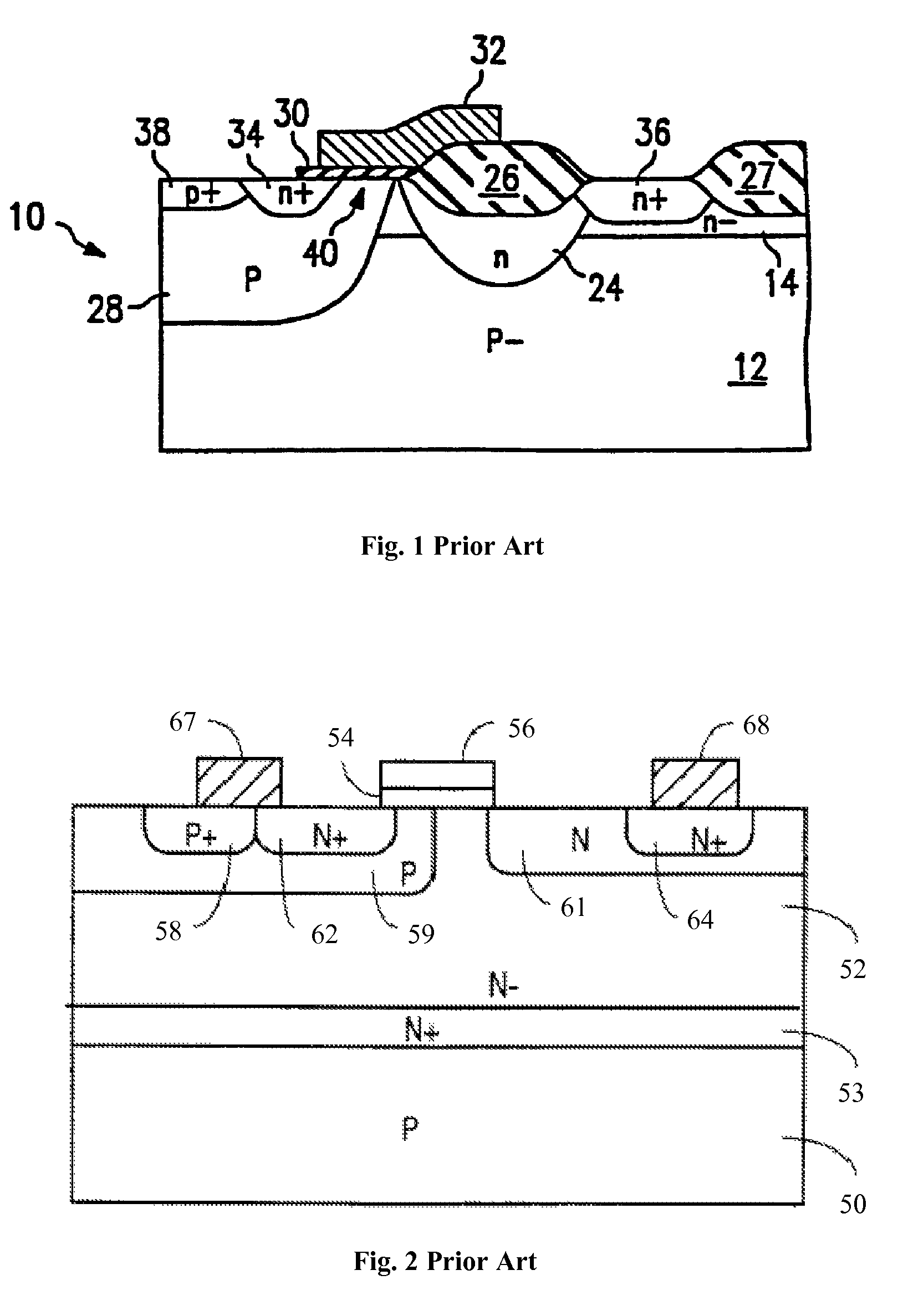
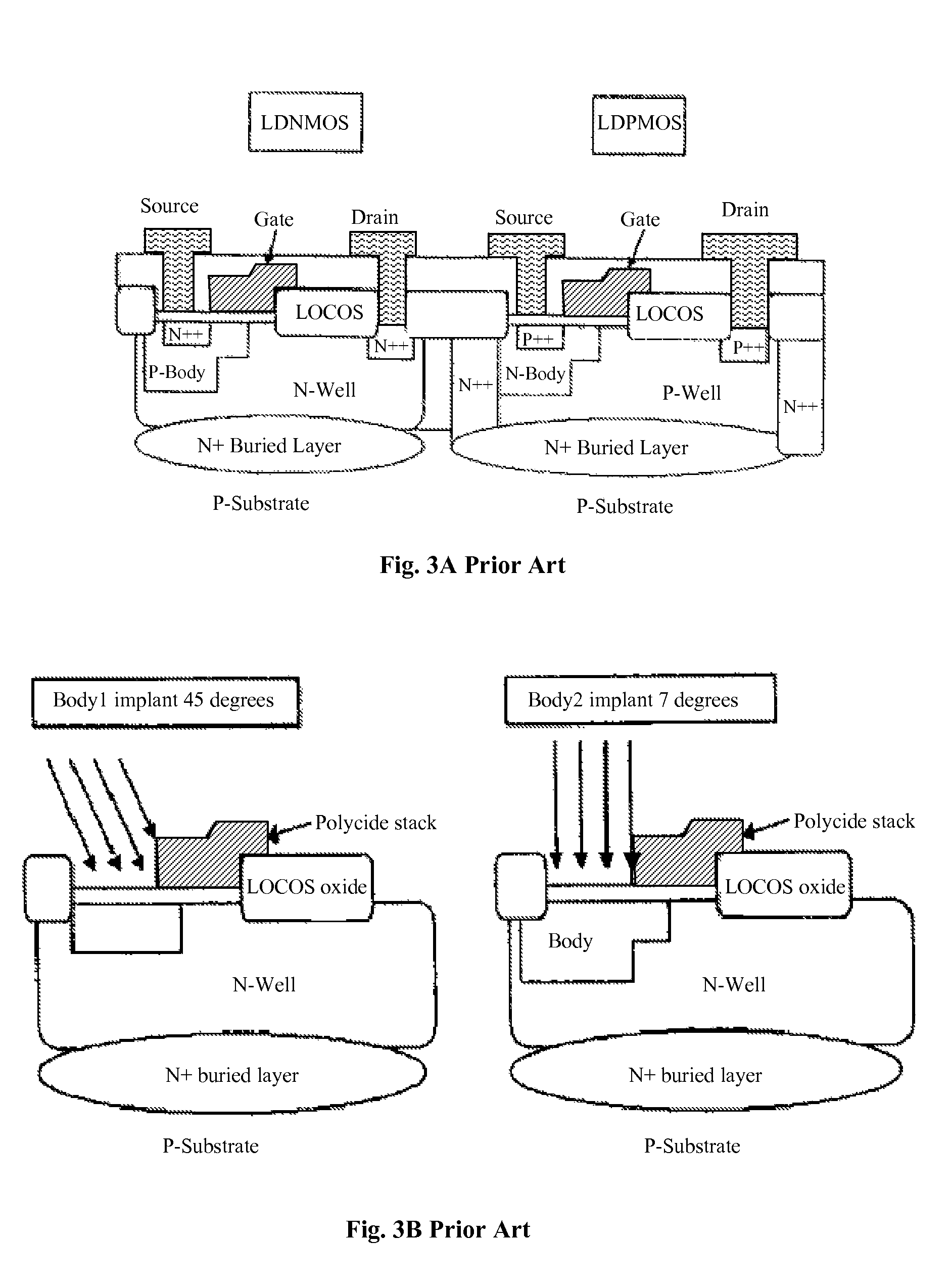
Embodiment Construction

[0078]The description above and below plus the drawings contained herein merely focus on one or more currently preferred embodiments of the present invention and also describe some exemplary optional features and / or alternative embodiments. The description and drawings are presented for the purpose of illustration and, as such, are not limitations of the present invention. Thus, those of ordinary skill in the art would readily recognize variations, modifications, and alternatives. Such variations, modifications and alternatives should be understood to be also within the scope of the present invention.

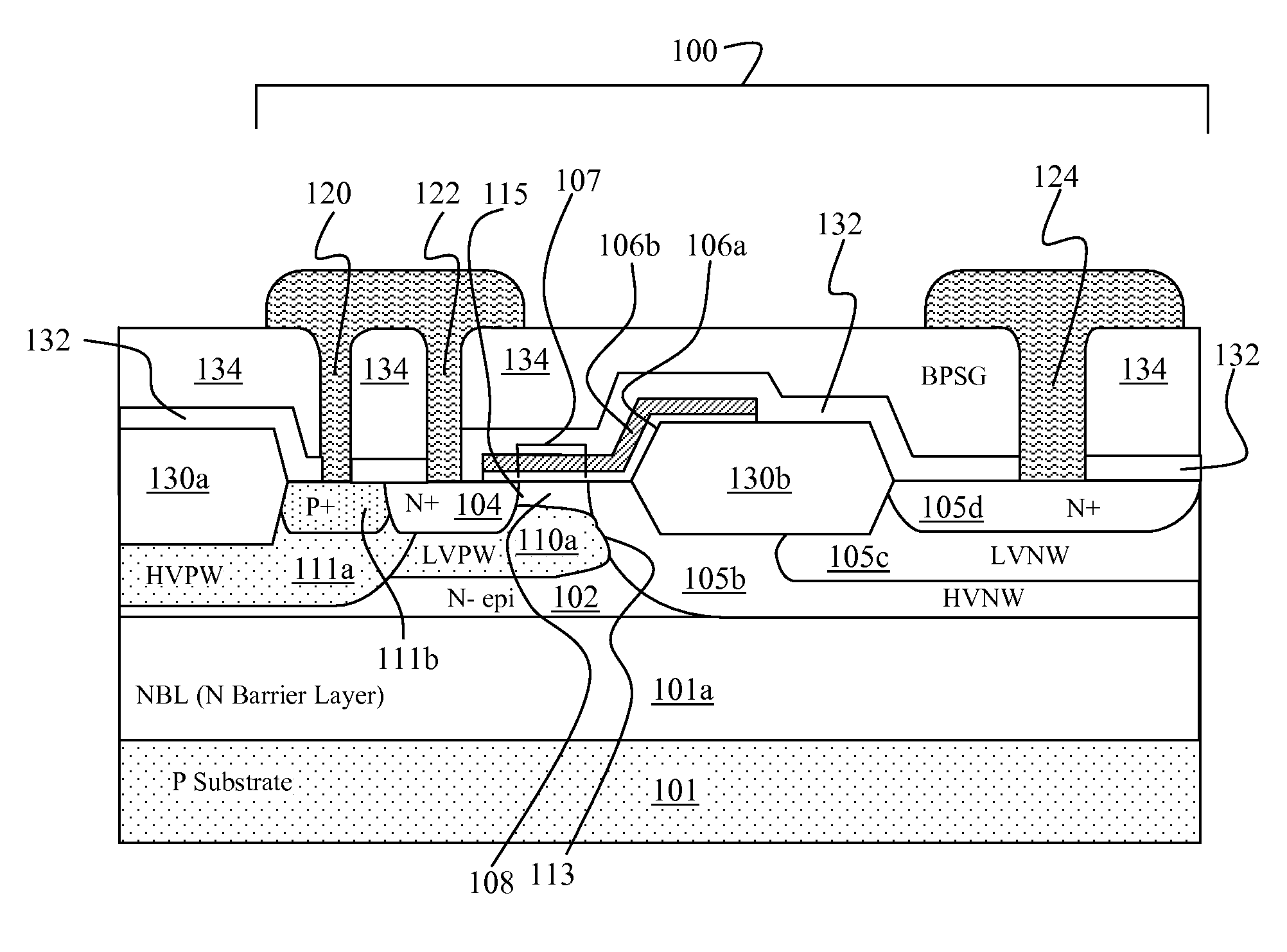
[0079]To simplify the graphical presentation of the fabrication process for the short channel LMOS device, the following convention of abbreviation known in the art is employed:

LV well implant=an implanted well for low voltage devices

HV well implant=an implanted well for high voltage devices

LVNW=an N-type well region for low voltage devices

LVPW=a P-type well region for low voltage devic...


PUM


Abstract

A short channel Lateral MOSFET (LMOS) and method are disclosed with interpenetrating drain-body protrusions (IDBP) for reducing channel-on resistance while maintaining high punch-through voltage. The LMOS includes lower device bulk layer; upper source and upper drain region both located atop lower device bulk layer; both upper source and upper drain region are in contact with an intervening upper body region atop lower device bulk layer; both upper drain and upper body region are shaped to form a drain-body interface; the drain-body interface has an IDBP structure with a surface drain protrusion lying atop a buried body protrusion while revealing a top body surface area of the upper body region; gate oxide-gate electrode bi-layer disposed atop the upper body region forming an LMOS with a short channel length defined by the horizontal length of the top body surface area delineated between the upper source region and the upper drain region.

Description

CROSS REFERENCE TO RELATED APPLICATIONS[0001]Not applicableFIELD OF INVENTION[0002]This invention relates generally to the field of power electronic device structure and fabrication. More specifically, the present invention is directed to a semiconductor device structure and fabrication method for improving its performance parameters.BACKGROUND OF THE INVENTION[0003]MOSFET (metal-oxide-semiconductor field effect transistor) devices have many industrial applications, such as power amplifiers, power switches, low noise amplifiers and digital Integrated Circuits (IC) to name a few. As a fundamental building cell for a great variety of electronic products, the practitioners in the art of MOSFET device design and fabrication are constantly improving its performance parameters such as power efficiency, maximum operating voltage, integration density and frequency response, to name a few.[0004]In U.S. Pat. No. 5,406,110 by Kwon, et al., a lateral double diffused insulated gate field effect ...

Claims


Application Information

Patent Timeline
Patent Type & Authority Patents(United States)
IPC IPC(8): H01L21/336H01L29/78
CPCH01L21/26513H01L21/26586H01L29/1095H01L29/66681H01L29/7816H01L29/0878H01L29/42368H01L2924/0002H01L2924/00
Inventor MALLIKARJUNASWAMY, SHEKARPAUL, AMIT
Owner ALPHA & OMEGA SEMICON INC
Why Eureka
Try Eureka