Laser exposure apparatus and laser annealing apparatus

a laser annealing and laser light technology, applied in the field of laser exposure apparatus, can solve the problem that the intensity distribution of laser light applied to the substance to be exposed cannot be homogenized, and achieve the effect of reducing coheren

Inactive Publication Date: 2010-12-14
FUJIFILM CORP
View PDF7 Cites 2 Cited by
  • Summary
  • Abstract
  • Description
  • Claims
  • Application Information

AI Technical Summary

Benefits of technology

[0010]In view of the above-described circumstances, the present invention is directed to provide a laser exposure apparatus and a laser exposure method, which allow, in a system using a multi-transverse mode semiconductor laser as a laser light source, reduction of coherency of the multi-transverse mode laser light and homogenization of intensity distribution of the laser light applied to a substance to be exposed.
[0011]The present invention is further directed to provide a laser annealing apparatus and a laser annealing method, which allow, in a system using a multi-transverse mode semiconductor laser as a laser light source, reduction of coherency of the multi-transverse mode laser light and homogenization of intensity distribution of the laser light applied to a substance to be exposed, thereby enabling uniform annealing of the substance to be exposed.

Problems solved by technology

Therefore, the intensity distribution of the laser light applied to the substance to be exposed cannot be homogenized simply by providing the optical homogenizing means in the optical path.
This is because that high-order transverse mode light of a certain order emitted by the multi-transverse mode semiconductor laser has two wavefront components that propagate in substantially symmetrical directions with respect to the optical axis, and the two wavefront components interfere with each other.

Method used


Image

  • Laser exposure apparatus and laser annealing apparatus
  • Laser exposure apparatus and laser annealing apparatus
  • Laser exposure apparatus and laser annealing apparatus

Examples


first embodiment

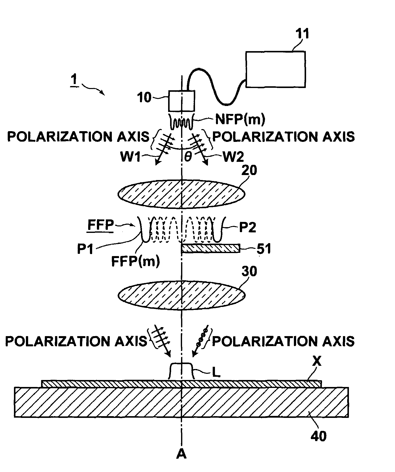
[0035]Now, referring to FIGS. 1A and 1B, the configuration of a laser exposure apparatus (laser annealing apparatus) according to a first embodiment of the present invention will be described.

[0036]The laser exposure apparatus 1 of this embodiment is an apparatus that applies laser light to a substance to be exposed X. The laser exposure apparatus 1 can be used, for example, as a laser annealing apparatus that anneals an amorphous or polycrystalline substance to be exposed X to improve crystal properties thereof. The laser exposure apparatus 1 can, for example, (1) polycrystallize an amorphous substance to be exposed X, (2) increase an average crystal diameter of a polycrystalline substance to be exposed X, or (3) single-crystallize a polycrystalline substance to be exposed X.

[0037]The substance to be exposed X is not particularly limited, and may be a film or a bulk body formed on a substrate. An example of the substance to be exposed X is an amorphous semiconductor film (having a ...

second embodiment

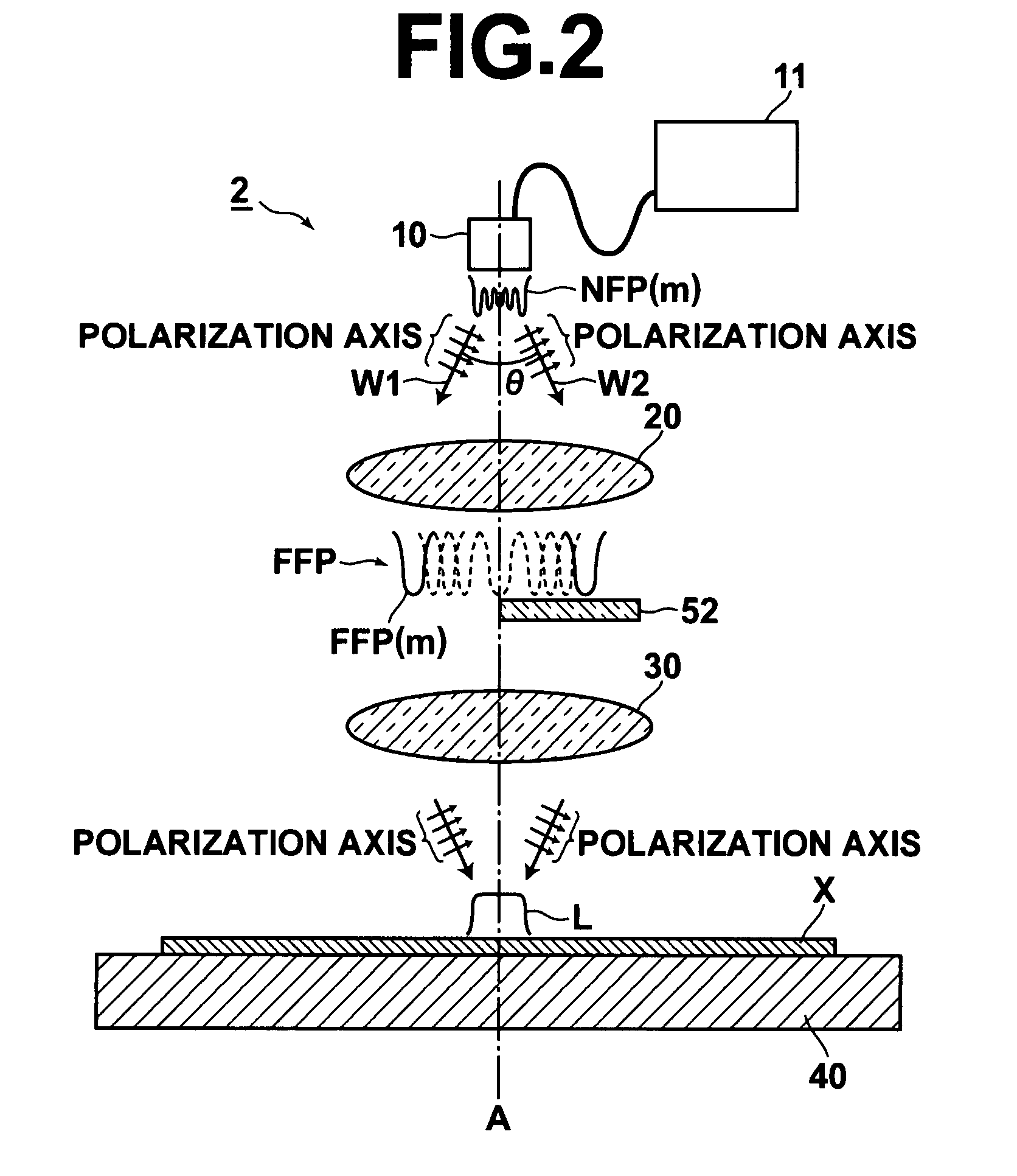
[0066]Next, referring to FIG. 2, a laser exposure apparatus (laser annealing apparatus) according to a second embodiment the invention will be described. Since the basic configuration of the apparatus of this embodiment is similar to that of the first embodiment, the same elements are designated by the same reference numerals and are not explained in detail.

[0067]The laser exposure apparatus (laser annealing apparatus) 2 of this embodiment includes, as the coherency reducing means for reducing coherency of the two wavefront components W1 and W2 contained in the high-order transverse mode light of each order, a translucent optical member 52 provided only in the optical path of the wavefront component W2, which is one of the two wavefront components W1 and W2. The translucent optical member 52 makes a difference in optical path length between the wavefront component W2 and the other wavefront component W1 not less than the coherence length of the laser light emitted from the laser lig...

third embodiment

[0076]Next, referring to FIG. 3, the configuration of a laser exposure apparatus (laser annealing apparatus) according to a third embodiment of the invention will be described. Since the basic configuration of the apparatus of this embodiment is similar to that of the first embodiment, the same elements are designated by the same reference numerals and are not explained in detail. FIG. 3A corresponds to FIG. 1A and FIG. 2, and FIG. 3B is a side view. In FIG. 3B, the transverse direction is a direction of the longitudinal mode of the laser light emitted from the laser light source 10.

[0077]In the laser exposure apparatus (laser annealing apparatus) 3 of this embodiment, as the coherency reducing means for reducing coherency of the two wavefront components W1 and W2 contained in the high-order transverse mode light of each order, a translucent optical member 53 is provided only in the optical path of the wavefront component W2, which is one of the two wavefront components W1 and W2. T...


PUM

PropertyMeasurementUnit
thicknessaaaaaaaaaa
optical path lengthaaaaaaaaaa
coherence lengthaaaaaaaaaa

Abstract

A laser exposure which includes: a laser light source including a multi-transverse mode semiconductor laser; a far-field pattern forming optical system for forming a far-field pattern of multi-transverse mode laser light emitted from the laser light source; a condensing optical system for condensing the laser light emitted from the far-field pattern forming optical system and applying the condensed laser light to a substance to be exposed; and a coherency reducing element disposed in an optical path between the laser light source and the substance to be exposed, for reducing coherency of two wavefront components that are contained in high-order transverse mode light of each order emitted from the laser light source and propagate in substantially symmetrical directions with respect to the optical axis.

Description

BACKGROUND OF THE INVENTION[0001]1. Field of the Invention[0002]The present invention relates to a laser exposure apparatus and a laser exposure method, which use a laser light source formed by a multi-transverse mode semiconductor laser. The present invention also relates to a laser annealing apparatus and a laser annealing method, which use a laser light source formed by a multi-transverse mode semiconductor laser.[0003]2. Description of the Related Art[0004]In the field of thin film transistors (TFT), or the like, laser annealing is conducted, in which an amorphous semiconductor film, such as an amorphous silicon film, is exposed to laser light to be annealed, thereby obtaining the polycrystalline semiconductor film.[0005]As conventional laser light sources for use in laser annealing, excimer lasers have been widely used in view of high power and good light absorption by amorphous semiconductor films. In recent years, use of a solid-state laser or a semiconductor laser as the las...

Claims


Application Information

Patent Timeline
Patent Type & Authority Patents(United States)
IPC IPC(8): B23K26/06H01L21/268
CPCB23K26/0639B23K26/0648B23K26/0665B23K26/064
Inventor HIIRO, HIROYUKI
Owner FUJIFILM CORP
Why Eureka
Try Eureka