Multilayer substrate and manufacturing method thereof

a technology of multi-layer substrates and manufacturing methods, applied in the field of multi-layer substrates, can solve the problems of difficult to clearly identify the boundary between the insulating layers, and achieve the effects of reducing the occurrence of warpage, reducing the variation in the thickness of the insulating layer, and improving the pattern accuracy

Active Publication Date: 2011-01-11
TDK CORPARATION
View PDF62 Cites 25 Cited by
  • Summary
  • Abstract
  • Description
  • Claims
  • Application Information

AI Technical Summary

Benefits of technology

[0011]It is therefore an object of the present invention to provide a multilayer substrate and a manufacturing method thereof, which can offer a high degree of design freedom and arbitrary selection of optimal pattern shapes and variations required in various electronic elements.

Problems solved by technology

It may sometimes be difficult to clearly identify the boundary between the insulating layers due to lamination of the insulating layers of the same material, such as a case of laminating a build-up layer on another build-up layer.

Method used


Image

  • Multilayer substrate and manufacturing method thereof
  • Multilayer substrate and manufacturing method thereof
  • Multilayer substrate and manufacturing method thereof

Examples


first embodiment

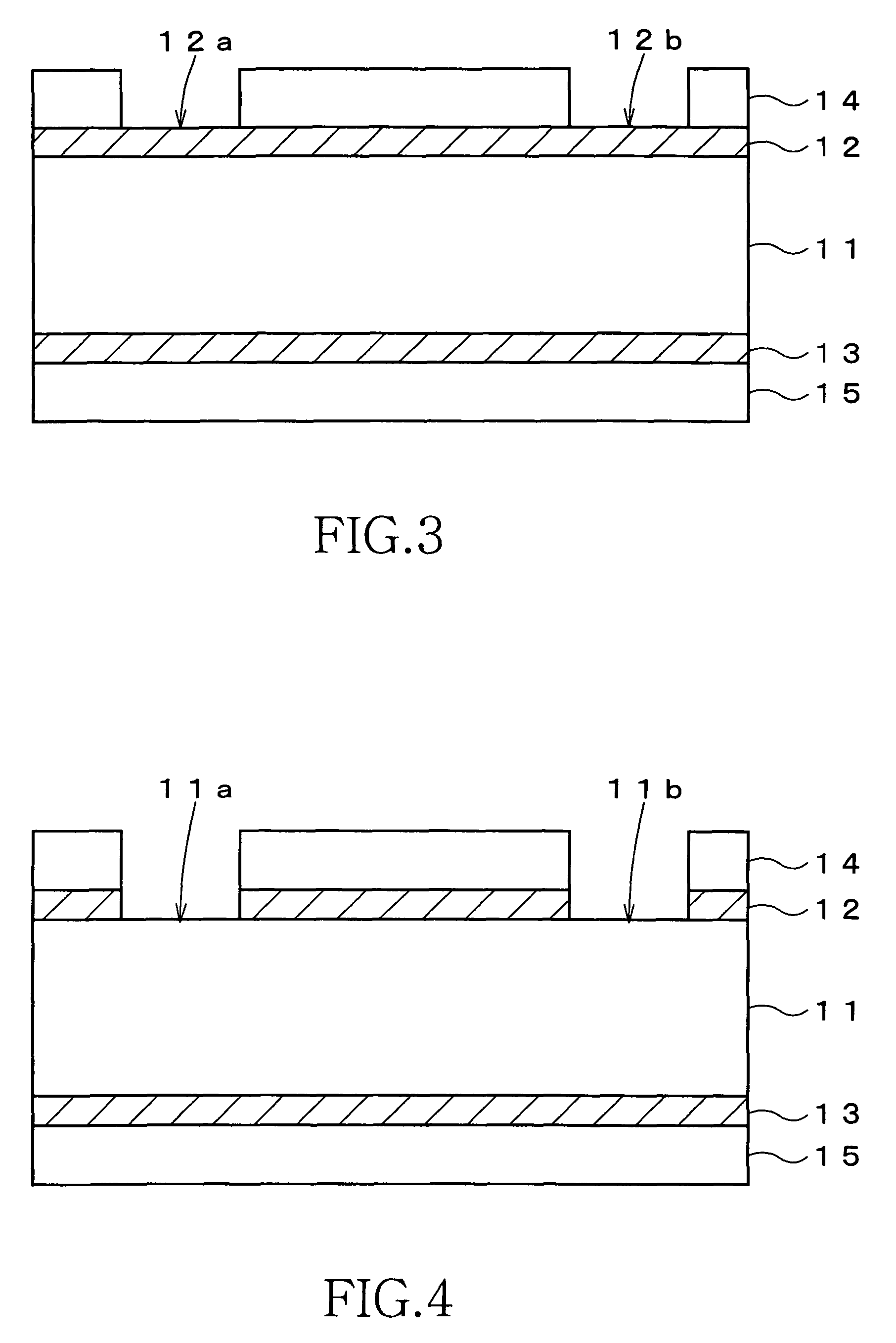
[0161]A method of manufacturing a multilayer substrate according to the present invention is applicable to both of a “core substrate” and a “build-up layer” to be provided on the core substrate, which constitutes the multilayer substrate. First, the case of applying the method of manufacturing a multilayer substrate according to the present invention to a “core substrate” will be described with reference to schematic cross-sectional views in FIG. 1 to FIG. 16.

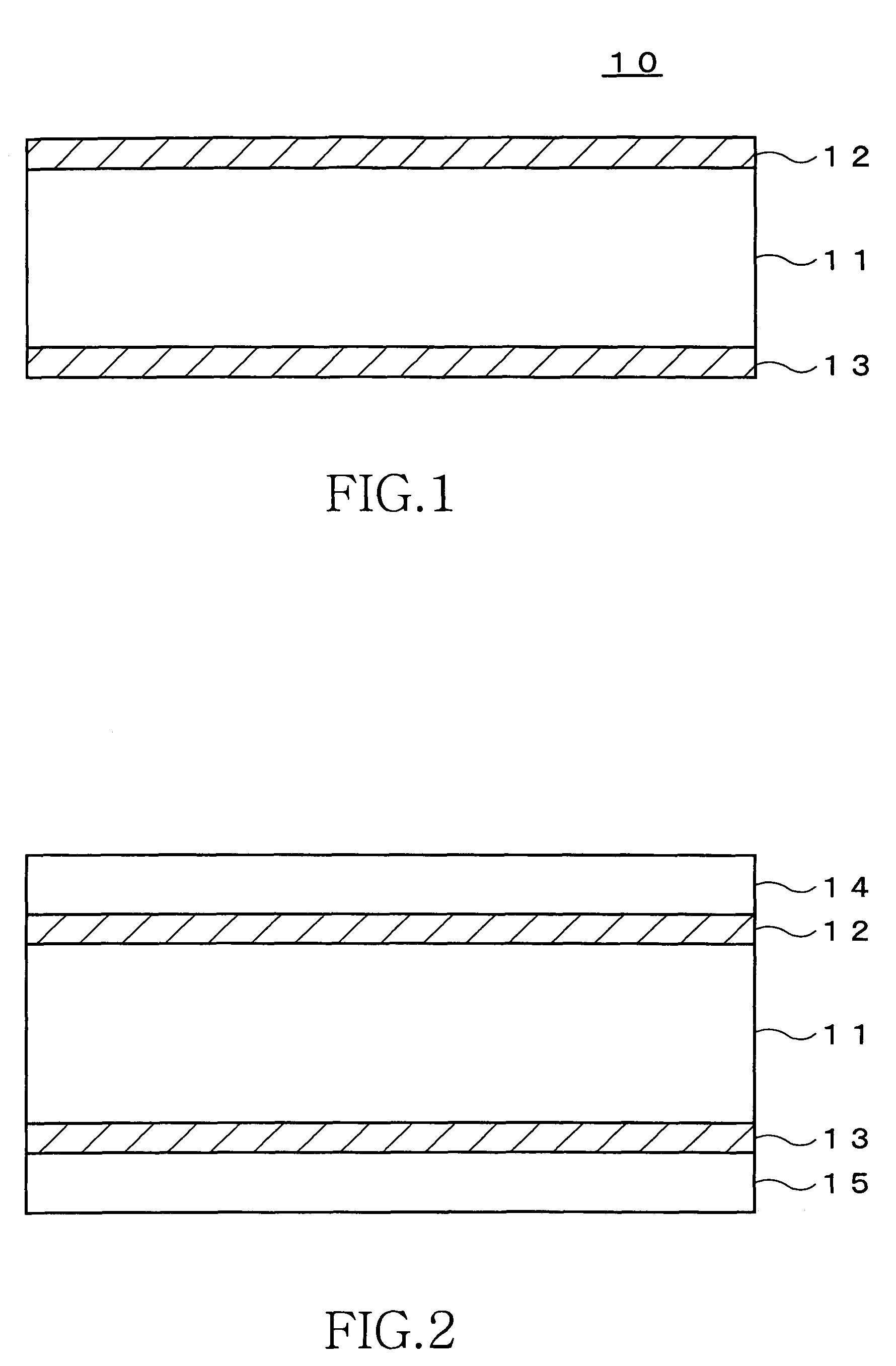
[0162]A core substrate 10 is prepared to begin with (FIG. 1). The core substrate 10 before processing includes an insulating layer 11, and conductive layers 12 and 13 respectively formed on both surfaces of the insulating layer 11. The insulating layer 11 serves to ensure overall mechanical strength upon fabrication of a multilayer substrate. Although the material of the insulating layer 11 is not particularly limited, it is preferable to use a core made of a glass cloth, Kevlar, a resin cloth such as liquid crystal polymer, a ...

second embodiment

[0193]Next, a method of manufacturing a multilayer substrate according to the present invention will be described in detail.

[0194]The method of manufacturing a multilayer substrate according to this embodiment is also applicable to both of a “core substrate” constituting a multilayer substrate and a “build-up layer” to be provided on the core substrate. In the following, the case of applying the method of manufacturing a multilayer substrate according to this embodiment to a “build-up layer” will be described with reference to schematic cross-sectional views in FIG. 38 to FIG. 51. Note that the basic processes for the core substrate are the same as the basic processes for the build-up layer as described in the first embodiment. Therefore, this embodiment will only describe application to the “build-up layer”, and will omit a description of application to the core substrate. In the meantime, the same constituents as those described in the first embodiment will be designated by the sa...

third embodiment

[0209]Next, the present invention will be described in detail.

[0210]A method of manufacturing a multilayer substrate according to this embodiment is also applicable to both of a “core substrate” constituting a multilayer substrate and a “build-up layer” to be provided on the core substrate. First, the case of applying the method of manufacturing a multilayer substrate according to this embodiment to a “core substrate” will be described with reference to schematic cross-sectional views in FIG. 52 to FIG. 62.

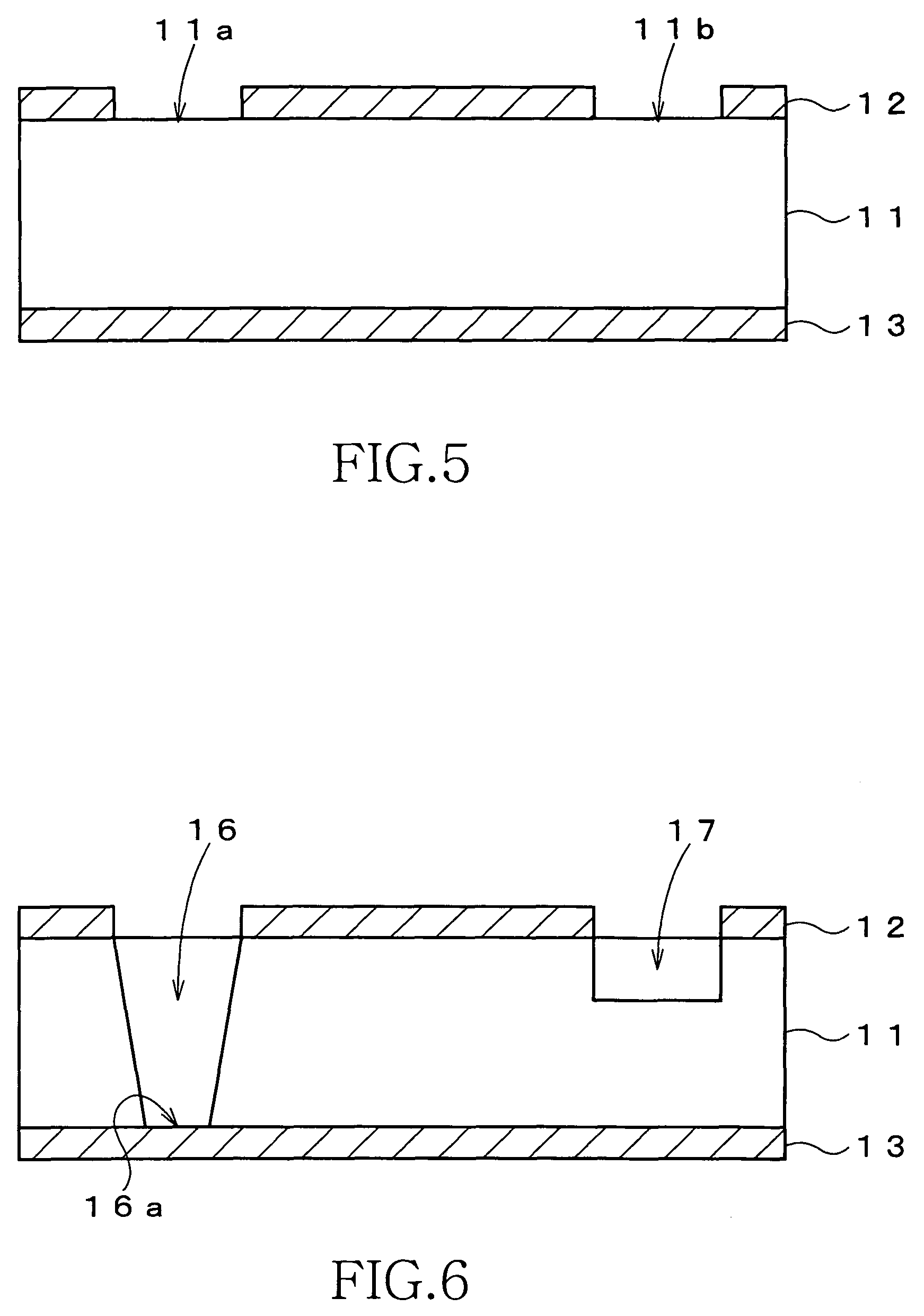
[0211]First, similarly to the first embodiment, a core substrate 10 is prepared and dry films 14 and 15 made of a photosensitive material are respectively attached to both surfaces of the core substrate 10 (FIG. 1 and FIG. 2). In this way, substantially the entire surfaces of conductive layers 12 and 13 are covered with the dry films 14 and 15. Thereafter, the dry films 14 and 15 are patterned by exposure and development processes to expose portions the conductive layers 12 and 13...


PUM

PropertyMeasurementUnit
thicknessaaaaaaaaaa
thicknessaaaaaaaaaa
thicknessaaaaaaaaaa

Abstract

A multilayer substrate according to the present invention includes a plurality of laminated insulating layers and conductive patterns formed between the respective insulating layers. The conductive patterns include a first conductive pattern having a predetermined thickness and a second conductive pattern thicker than the first conductive pattern. The first and second conductive patterns are located in the same layer. The first conductive pattern is formed by pattern-etching a conductive layer having a uniform thickness by the subtractive method. The second conductive pattern is formed by forming a pattern-forming groove and then filling the inside of the pattern-forming groove with a conductive material simultaneously with forming a via hole. The first conductive pattern is suitable for an LC pattern for a high-frequency circuit requiring small variations in the width and the thickness of the pattern as well as accuracy in the thickness relative to an insulating pattern, and for a normal conductive pattern requiring impedance matching. The second conductive pattern is suitable for an L pattern for a choke coil.

Description

TECHNICAL FIELD[0001]The present invention relates to a multilayer substrate and a manufacturing method thereof. More specifically, the present invention relates to a multilayer substrate including a conductive pattern and a via hole electrode, and a manufacturing method thereof.BACKGROUND OF THE INVENTION[0002]The need for higher-density packaging becomes increasingly severe in recent years. For this reason, “multilayer substrates” including lamination of a plurality of insulating layers are often used as substrates for various modules to be mounted on printed circuit boards.[0003]A typical multilayer substrate is manufactured by forming conductive patterns and other elements on respective insulating layers collectively constituting the multilayer substrate, and then laminating the insulating layers together. Connection between the conductive patterns formed on the different insulating layers is achieved by use of via holes penetrating the insulating layers (see Japanese Patent No....

Claims


Application Information

Patent Timeline
Patent Type & Authority Patents(United States)
IPC IPC(8): H01L23/485
CPCC25D5/022H05K3/107H05K1/0265Y10T428/24917H05K3/0032H05K3/06H05K3/064H05K3/108H05K3/20H05K3/243H05K3/421H05K3/4652H05K2201/0355H05K2201/0376H05K2201/0394H05K2201/09036H05K2201/09563H05K2201/096H05K2201/09736H05K2203/0384H05K2203/0542H05K2203/1476
Inventor KAWABATA, KENICHIABE, HISAYUKIKATSUMATA, MASASHI
Owner TDK CORPARATION
Why Eureka
Try Eureka