Mounting structure and electro optical device

a technology of mounting structure and electro optical device, which is applied in the direction of identification means, semiconductor/solid-state device details, instruments, etc., can solve the problems of increasing wiring resistance and not being able to avoid the reduction of width, and achieve good electrical connection

Active Publication Date: 2011-01-11
SEIKO EPSON CORP
View PDF3 Cites 10 Cited by
  • Summary
  • Abstract
  • Description
  • Claims
  • Application Information

AI Technical Summary

Benefits of technology

[0010]An advantage of some aspects of the invention is to provide a mounting structure which makes it possible to provide a good electrical connection between a substrate-side terminal and a component-side terminal even when the number of wiring pattern and the number of substrate-side terminal are increased without extending a mounting area, and to provide an electro optical device equipped with the same.
[0019]In addition, the width size Wa1 of the substrate-side first terminal that is located at a portion to which the substrate-side first wirings and the substrate-side second wirings are extended is narrower than the width size Wa2 of the substrate-side second terminal. Consequently, the substrate-side second wiring pattern can be easily passed trough between the substrate-side first terminals, and shortcut between the substrate-side second wiring pattern and the substrate-side first terminal and occurrence of overlapping of the substrate-side second wiring pattern and the substrate-side first terminal are prevented. Accordingly, at the side of the substrate, even when the number of the wiring pattern and the substrate-side terminal is increased without extending the mounting area, it is not necessary to purposely narrow the width sizes. Further, there is no substrate-side first terminal at a position adjacent to the substrate-side second terminal in the Second direction, so that the substrate-side second terminal can be formed to have an enough width size. Consequently, even when the pitch of the substrate-side first terminals and the pitch of the substrate-side second terminals are narrowed in order to increase the number of the wiring pattern and the substrate-side terminal without extending the mounting area, a problem such as shortcut does not occur. Further, the width size of the component-side first terminal that is connected to the substrate-side first terminal at the side of the component is increased as the width size of the substrate-side first terminal is narrow. On the other hand, the width size of the component-side second terminal that is connected to the substrate-side second terminal at the side of the component is decreased as the width size of the substrate-side second terminal is wide. Consequently, even when the width size of each of the terminals is narrowed, the substrate-side first terminal surely overlaps with the component-side first terminal, and the substrate-side second terminal surely overlaps with the component-side second terminal, so that electrical connection is assured. In addition, the overlapped area of the substrate-side first terminal and the component-side first terminal and the overlapped area of the substrate-side second terminal and the component-side second terminal are equivalent. Consequently, there is an advantage that, for example, the connection resistance of each connection part is equivalent, so that the resistance value of each signal transmission pathway between the substrate and the component is equivalent.
[0021]That is, as for the substrate-side second terminals, there is a special allowance in the Second direction perpendicular to the first direction. Accordingly, as for the substrate-side second terminals, the width size can be increased than that of the substrate-side second wirings. Accordingly, reliability of an electrical connecting part with the component can be improved.
[0023]That is, as for the substrate-side first terminals, there is no special allowance in the Second direction. However, it is preferable that the width size of the substrate-side first terminal is formed so as to be equivalent to the substrate-side first wiring pattern and the width size is increased to the utmost limit. With the structure, reliability of an electrical connecting part with the component can be improved.

Problems solved by technology

Consequently, when the number of the wirings and the number of the substrate-side terminals is increased without extending the mounting area 10j in the Second direction, there is a problem in that it can not be avoided to decrease the width size of the substrate-side second wirings 192, which increases the wiring resistance.

Method used


Image

  • Mounting structure and electro optical device
  • Mounting structure and electro optical device
  • Mounting structure and electro optical device

Examples


first embodiment 1

Whole Structure

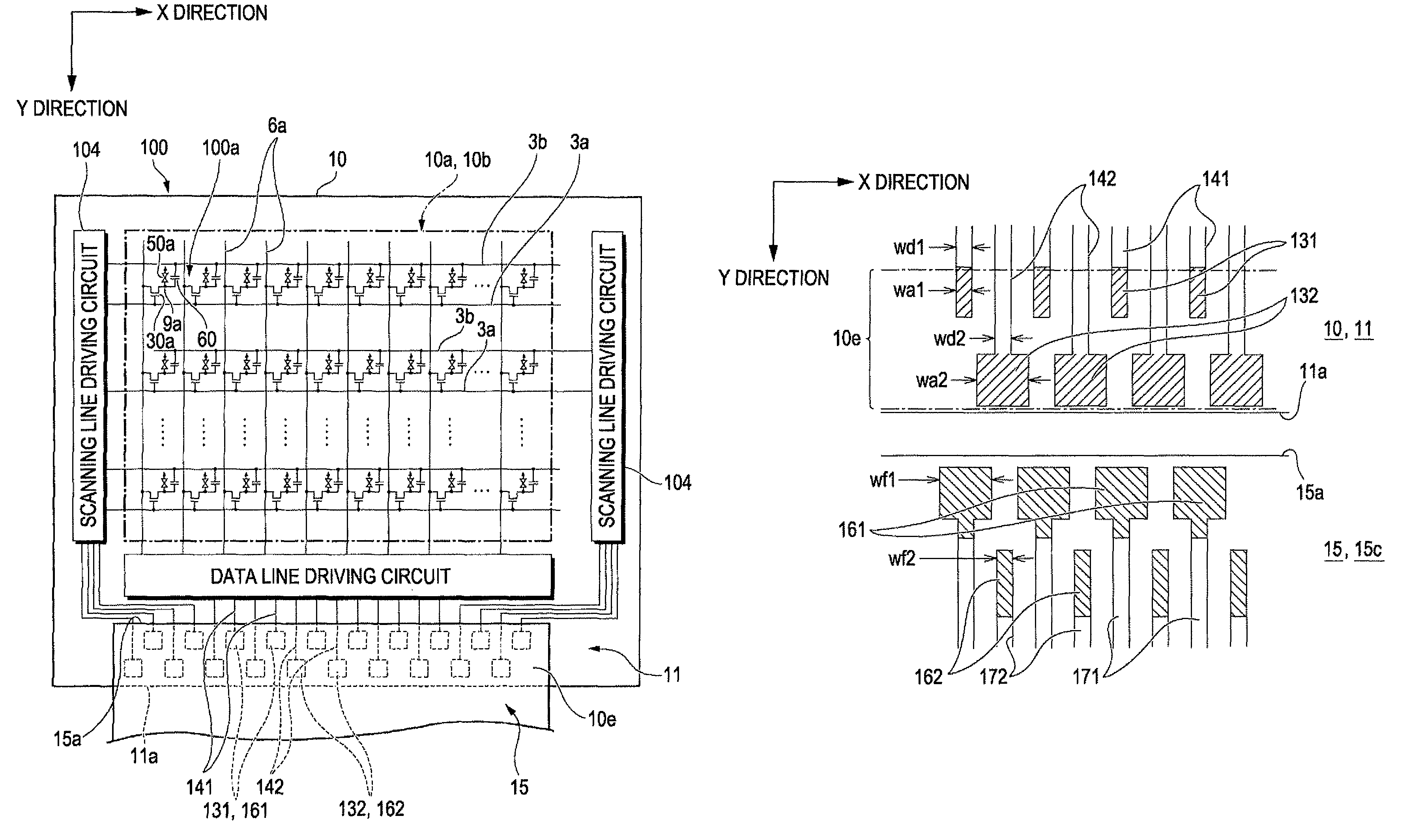
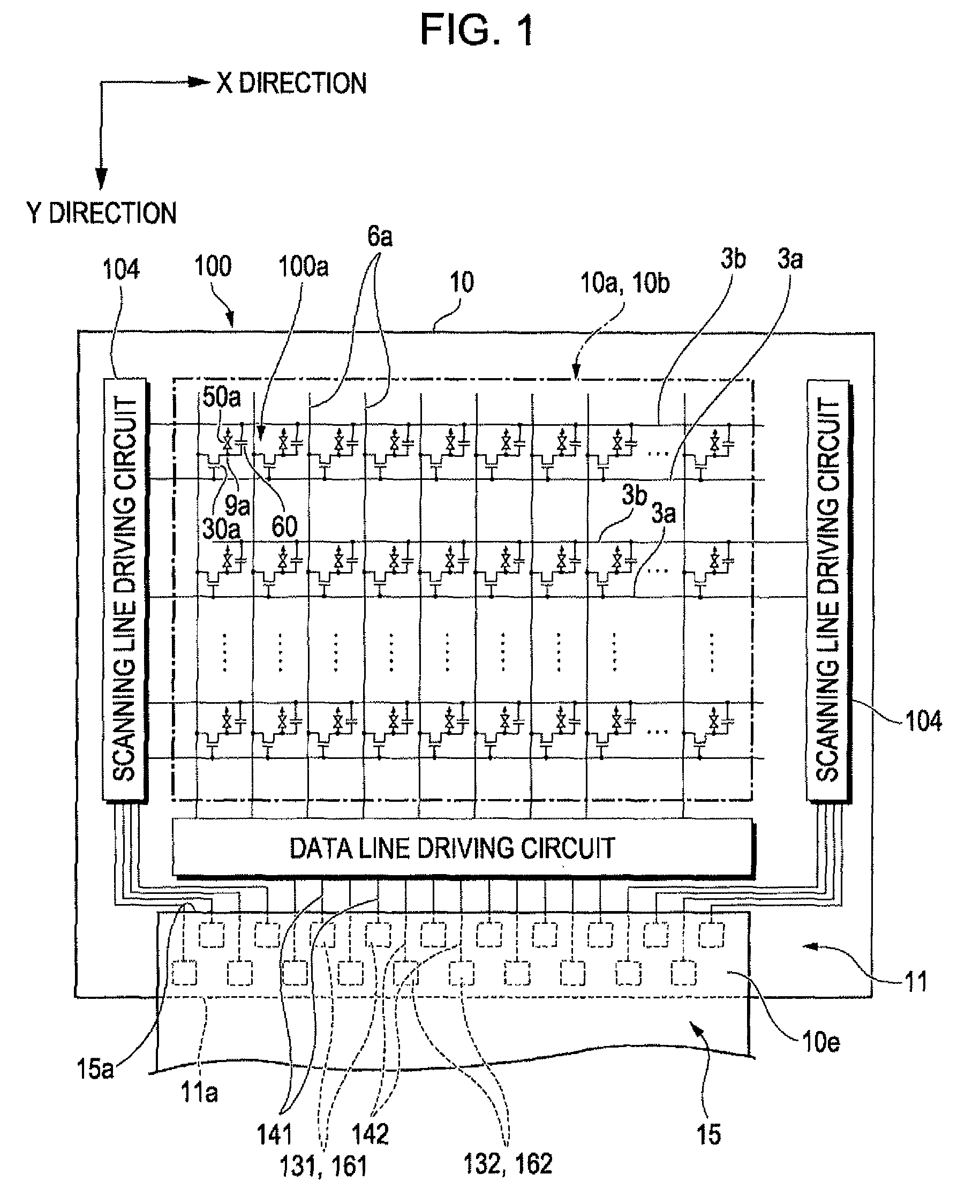
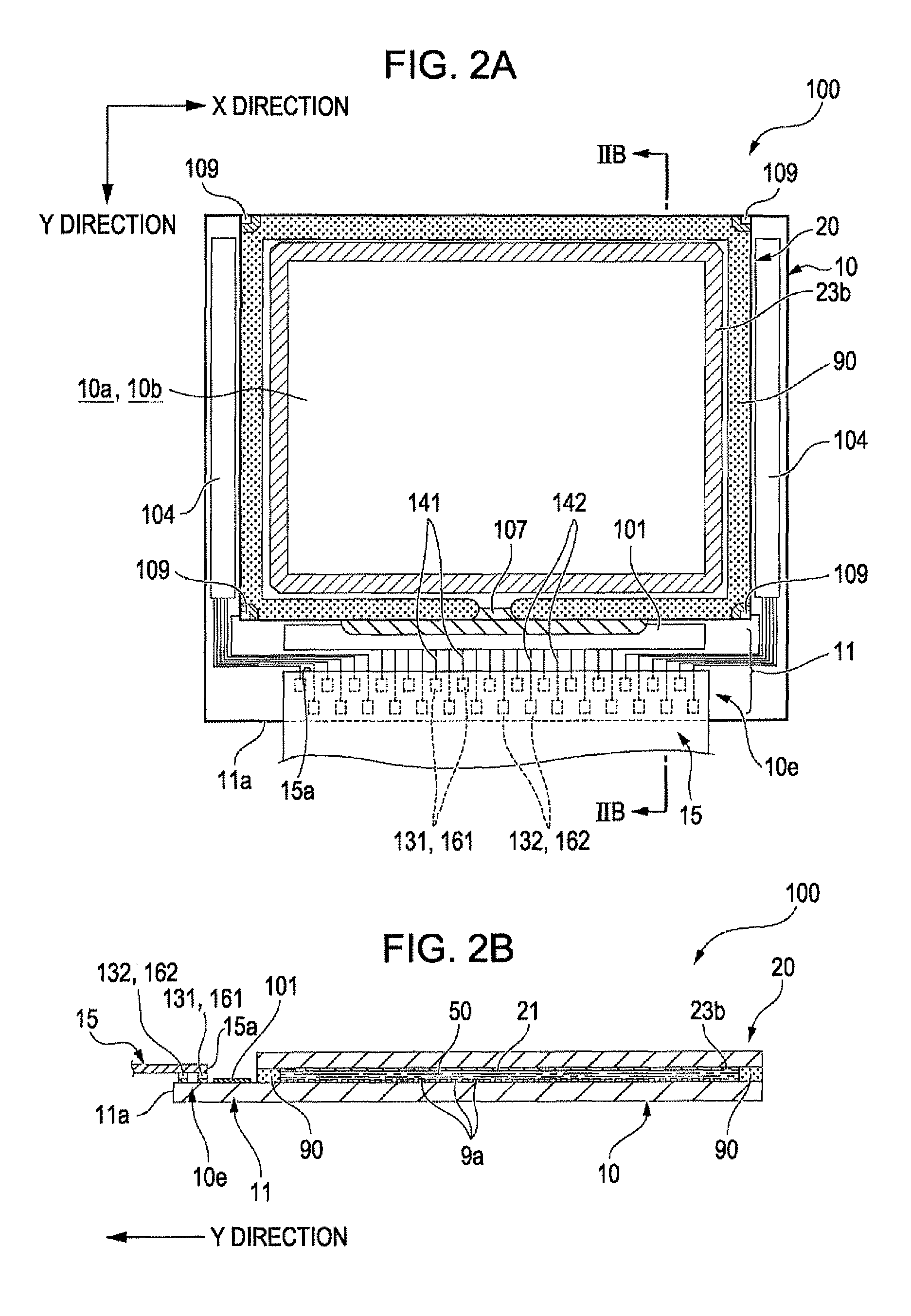
[0051]FIG. 1 is an equivalent circuit diagram showing an electrical structure of a first substrate (element substrate / electro optical device substrate) used in an electro optical device (liquid crystal device) according to a first embodiment of the invention. FIG. 2A is a plan view showing the electro optical device according to the first embodiment of the invention viewed from a side of a counter substrate with each constituent element formed thereon, and FIG. 2B is a cross sectional view thereof taken along the line IIB-IIB of FIG. 2A.

[0052]As shown in FIG. 1, an electro optical device 100 according to the embodiment is a liquid crystal device, and a plurality of pixels 100a are formed in a pixel area 10b in a matrix manner. A pixel electrode 9a and a thin film transistor 30a (pixel transistor) for pixel switching for controlling the pixel electrode 9a are formed in each of the plurality of the pixel electrodes 100a. Further, a data line driving circuit 101 and scan...

embodiment

Main Effect of Embodiment

[0075]FIG. 5 is an explanatory diagram schematically showing a planer structure when the positional relationship between the first substrate 10 and the flexible printed circuit 15 is deviated in the Second direction in the mounting are 10e shown in FIG. 3B.

[0076]As described above, in the electro optical device 100 of the embodiment, the first substrate 10 and the flexible printed circuit 15 constitute a mounting structure. In the mounting structure, the plurality of substrate-side first terminals 131 and the plurality of substrate-side second terminals 132 that are aligned in the Second direction are arranged in two rows in the First direction. Further, the substrate-side first terminals 131 and the substrate-side second terminals 132 are formed at positions deviated in the Second direction. Also in the flexible printed circuit 15, the plurality of component-side first terminals 161 and the component-side second terminals 162 are arranged in two rows in the...

second embodiment

[0088]FIG. 6A is a plan view showing an electro optical device (liquid crystal device) according to a second embodiment of the invention viewed from a side of a counter substrate with each constituent element formed thereon, and FIG. 6B is a cross sectional view thereof taken along the line VIB-VIB of FIG. 6A. FIG. 7A is an explanatory diagram schematically showing a planer structure of wirings and terminals formed in a projected area of the first substrate 10 and a driving IC, and FIG. 7B is an explanatory diagram schematically showing a planer structure of an appearance when the driving IC is overlapped with the projected area of the first substrate 10 and the terminals thereof are electrically connected to each other, in the electro optical device according to the second embodiment of the invention. An end among the mounting area of the driving IC at the pixel area side is magnified in FIGS. 7A, 7B. FIG. 8A is an explanatory diagram schematically showing a cross sectional structu...


PUM

PropertyMeasurementUnit
areaaaaaaaaaaa
widths Wa1aaaaaaaaaa
width Wa1aaaaaaaaaa

Abstract

In a mounting structure in which a component is mounted on a substrate, substrate-side first wirings, substrate-side first terminals formed in a mounting area where the component is mounted on the substrate, substrate-side second terminals formed in the mounting area and substrate-side second wirings are disposed over the substrate. Component-side first terminals and component-side second terminals are provided to the component.

Description

BACKGROUND[0001]1. Technical Field[0002]The present invention relates to a mounting structure in which a component such as a flexible printed circuit, an IC, or the like is mounted on a substrate, and to an electro optical device equipped with the same.[0003]2. Related Art[0004]A pixel is formed at a position corresponding to each intersection point of a number of data lines and a number of scanning lines, and a predetermined signal is supplied to each pixel via the data lines and the scanning lines to drive each pixel in an active matrix liquid crystal device, an organic electro-luminescence display device, and an electro optical device such as a plasma display. Accordingly, in the electro optical device, a structure is employed in which a component such as a driving IC, a flexible printed circuit, or the like is mounted on a substrate for holding an electro optical material (for example, see JP-A-2003-66480).[0005]When mounting such a component, as shown in FIG. 12A, when perpendi...

Claims


Application Information

Patent Timeline
Patent Type & Authority Patents(United States)
IPC IPC(8): G02F1/1345H01J11/02G09F9/00G09F9/30H05K1/14
CPCH05K1/111H05K3/361G02F1/1345H01L23/49838H01L2924/0002H01L23/4985H05K1/112H05K1/117H05K3/323H05K2201/09427H05K2201/09436H05K2201/09709H05K2201/10674H01L2924/00Y02P70/50G02F1/133
Inventor YOKOTA, TOMOKI
Owner SEIKO EPSON CORP
Why Eureka
Try Eureka