Coupling device with compensated birefringence

a birefringence and coupling device technology, applied in the field of coupling devices, can solve the problems of optical fibers not being directly connected to a planar waveguide, optical fibers cannot be directly connected to a waveguide, and the optimal angle of incidence for coupling light is different, so as to increase the coupling ratio of the coupling device

Inactive Publication Date: 2011-02-01
COMMISSARIAT A LENERGIE ATOMIQUE ET AUX ENERGIES ALTERNATIVES
View PDF13 Cites 7 Cited by
  • Summary
  • Abstract
  • Description
  • Claims
  • Application Information

AI Technical Summary

Benefits of technology

[0033]The particular structuring of the first layer makes it possible to render the coupling device insensitive to polarization while compensating for the birefringence of said first layer.
[0050]The optical coupling device further advantageously includes a reflecting structure placed between the support substrate and the first layer, this reflecting structure being chosen from amongst a Bragg mirror, a layer of metal or a photonic crystal layer. The presence of this reflecting layer makes it possible to increase the coupling ratio of the coupling device.

Problems solved by technology

The problem is that the dimensions of the cross-section of an optical fiber remain large (from ten to a few tens of micrometers) in comparison with the cross-section of the planar waveguides.
Therefore, optical fibers cannot be directly connected to a planar waveguide, but are connected by a device called a coupling device.
The disadvantage of this solution is that the optimal angle of incidence θ for coupling the light is different for the two polarizations.
This problem is inherent to the asymmetry of the cross-section of planar waveguides.
It is therefore impossible to directly connect a planar optical waveguide to an optical fiber.
Thus, not only does the solution proposed in document [1] have the disadvantage of doubling the complexity of the final device, but, in addition, for reasons of symmetry, the two nanophotonic circuits 350, 340 must be completely identical.

Method used


Image

  • Coupling device with compensated birefringence
  • Coupling device with compensated birefringence
  • Coupling device with compensated birefringence

Examples


Embodiment Construction

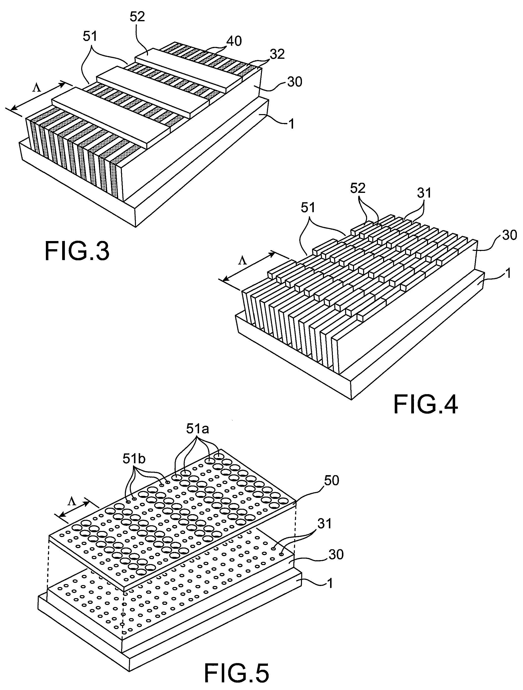
[0077]As see above, the coupling device, according to the chosen patterns, can have various configurations.

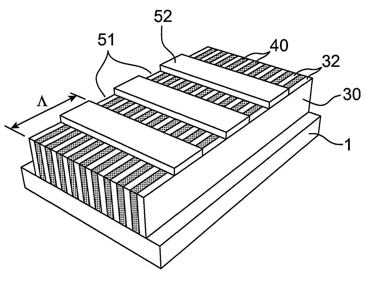
[0078]As shown in FIG. 3, the first layer 30 can include slots of uniform width spaced apart periodically, the slots passing through the entire thickness of the first layer. For example, the first layer can have a thickness of 220 nm, the width of the slots being 80 nm and the period between the slots being 120 nm. In FIG. 3, the slots produced in the first layer 30 are filled in with a different material: strips 32 and strips 40 made of different materials are thus obtained.

[0079]As regards the second layer, it likewise includes slots 51 of uniform width, which are spaced apart periodically and arranged perpendicular to the slots of the first layer. In this way, strips 52 perpendicular to strips 32 are obtained. The second layer, for example, can have a thickness of 150 nm, the width of the slots 51 being 300 nm and the period between the slots being 400 nm.

[0080]It is noted t...


PUM

PropertyMeasurementUnit
widthaaaaaaaaaa
widthaaaaaaaaaa
wavelengthaaaaaaaaaa

Abstract

The invention relates to a coupling device comprising a support substrate; a first layer arranged on the support substrate and comprising first patterns produced within the thickness of said first layer, said first patterns being arranged in parallel and periodic rows; a second layer arranged on the first layer and comprising second patterns passing through the thickness of said second layer, said second patterns being arranged in parallel and periodic rows. The direction of periodicity of the rows of the first patterns is perpendicular to the direction of periodicity of the rows of the second patterns. The rows of the first patterns extend over a distance greater than or equal to the wavelength in the void of the optical wave intended to be coupled. The first patterns have a width less than or equal to a tenth of the wavelength of the optical wave intended to be coupled, and the period of these patterns is between 50 nm and 1 μm. The second patterns are arranged so as to form a periodic diffraction grating.

Description

TECHNICAL FIELD[0001]The invention relates to a coupling device, as well as to the manufacturing method thereof, the coupling device being polarization-insensitive.PRIOR ART[0002]In the field of optoelectronics, planar optical waveguides are widely used.[0003]In these planar optical waveguides, it is indeed possible to produce complex optical beam management functions such as multiplexing, demultiplexing, modulation, spectral routing . . . .[0004]These functions can also be dedicated to both very short-distance optical links, on the scale of a millimeter (e.g., as for intra-chip communication), as well as to very long-distance optical links, of the order of several km (e.g., as in the metropolitan area network).[0005]It is possible to integrate a high density of such optical functions compactly, on a single chip. To accomplish this, it is necessary to miniaturize the optical circuits, which results in likewise miniaturizing the cross-section of the optical waveguides, in which the o...

Claims


Application Information

Patent Timeline
Patent Type & Authority Patents(United States)
IPC IPC(8): G02B6/34C23F1/00H01L21/00G02B6/10G02B6/30
CPCB82Y20/00G02B5/1809G02B5/1814G02B6/1225G02B6/34G02B6/30G02B5/3083
Inventor BEN BAKIR, BADHISETCHELNOKOV, ALEXEI
Owner COMMISSARIAT A LENERGIE ATOMIQUE ET AUX ENERGIES ALTERNATIVES
Why Eureka
Try Eureka