Self-aligned epitaxially grown bipolar transistor

a bipolar transistor and self-aligning technology, applied in the field of semiconductor processing, can solve the problems of affecting device performance, reducing the rf performance of bipolar transistors, so as to minimize the parasitic collector-base (ccb) and emitter-base (ceb) capacitance and minimize the base resistance rb-ext

Active Publication Date: 2011-02-08
NXP BV
View PDF3 Cites 7 Cited by
  • Summary
  • Abstract
  • Description
  • Claims
  • Application Information

AI Technical Summary

Benefits of technology

[0013]There exists a continuous need to minimize the parasitic collector-base (CCB) and emitter-base (CEB) capacitance of a bipolar transistor and to minimize the base resistance RB-ext. Furthermore, the process should be compatible with CMOS recipes and not require too many additional steps.

Problems solved by technology

As the number of electronic devices per given area of the silicon wafer increases, the manufacturing process becomes more difficult.
RF performance of bipolar transistors is largely limited by parasitics.
Such parasitics negatively affect device performance.

Method used


Image

  • Self-aligned epitaxially grown bipolar transistor
  • Self-aligned epitaxially grown bipolar transistor
  • Self-aligned epitaxially grown bipolar transistor

Examples


Embodiment Construction

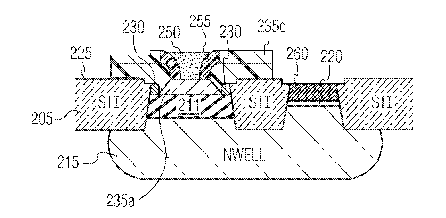
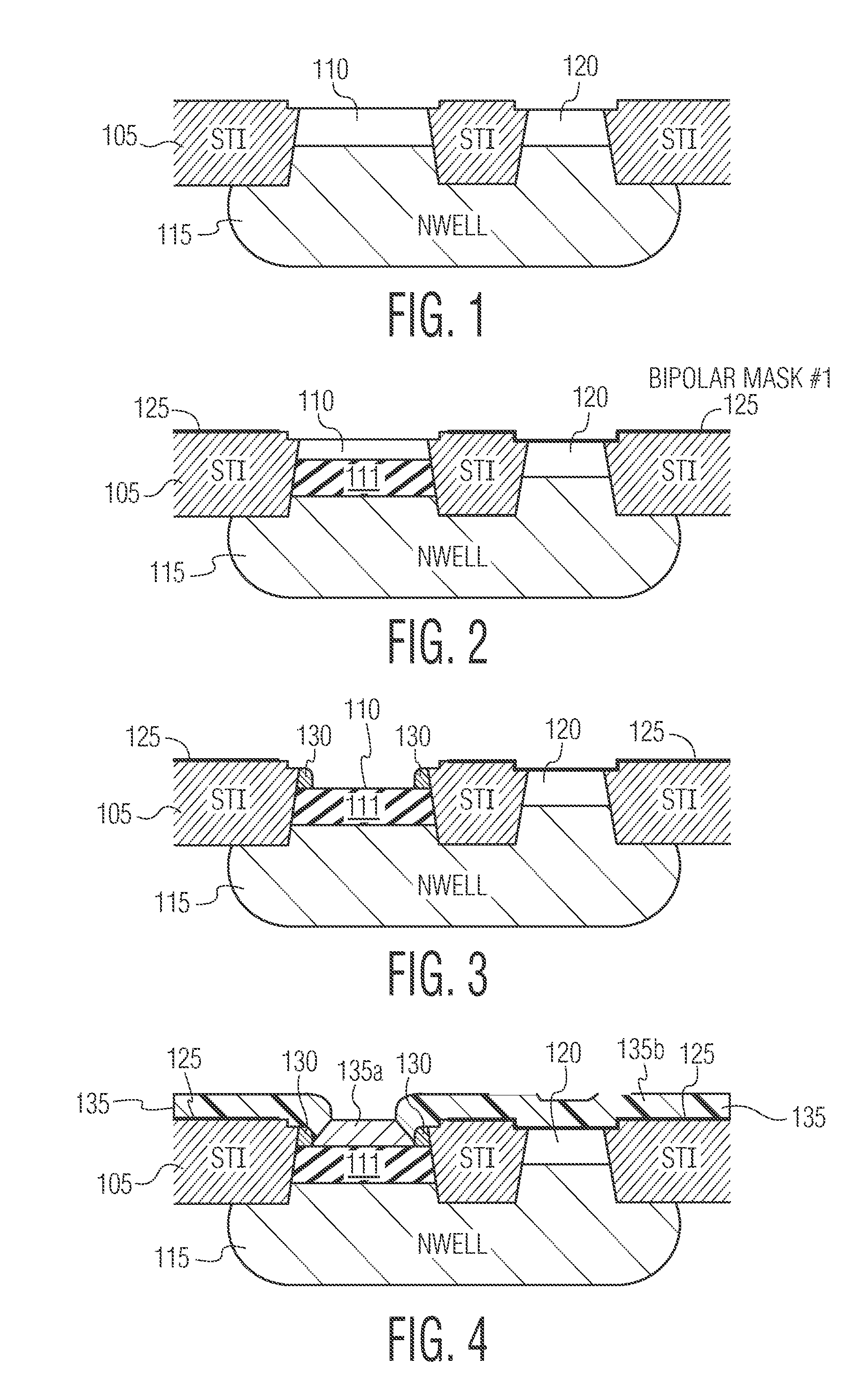
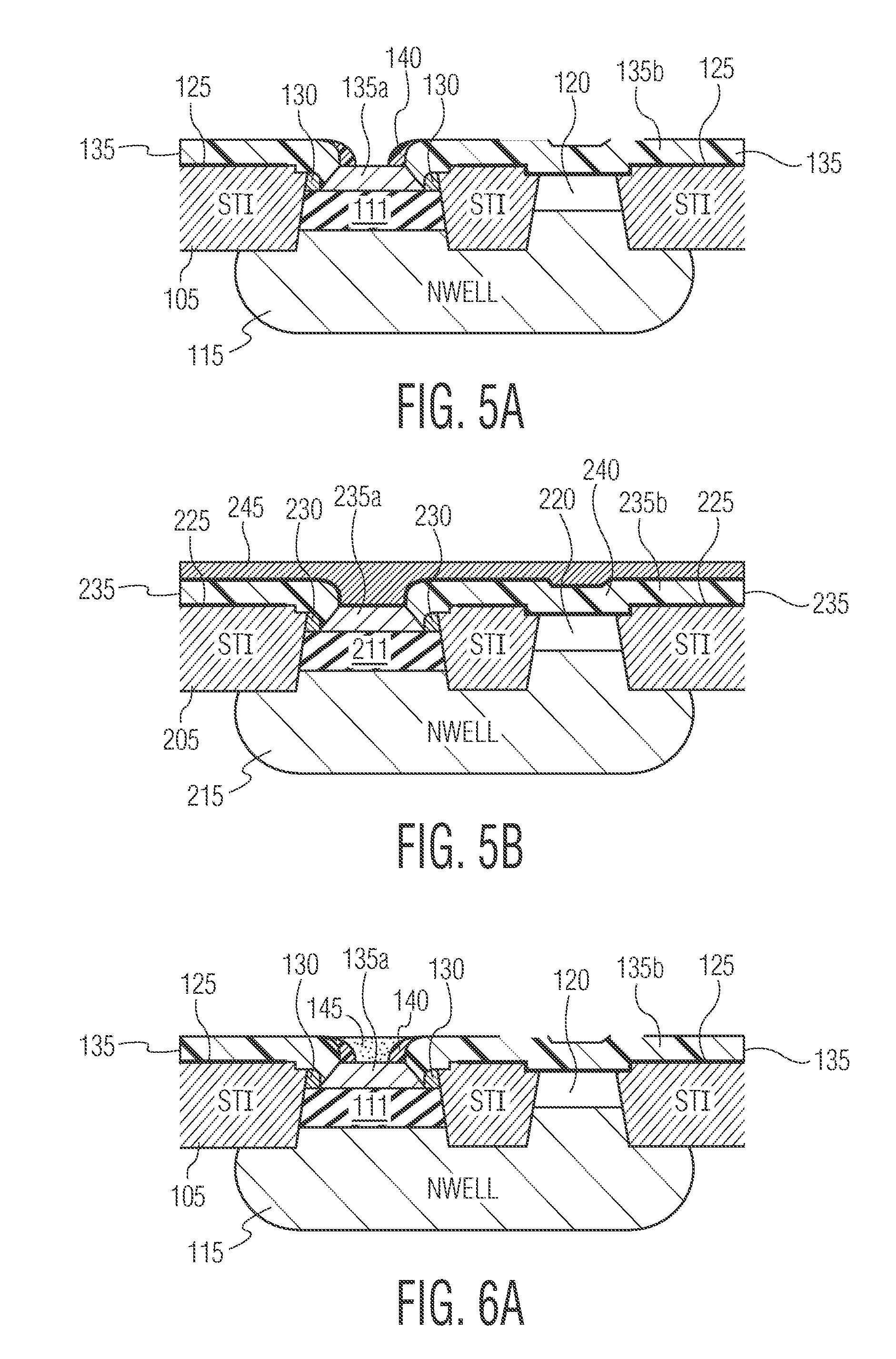
[0026]The present invention has been found useful in the fabrication of a bipolar transistor, or a SiGe hetero-junction bipolar transistor (HBT), in a fully self-aligned manner, which is compatible with standard CMOS processing. Hence, this structure is suitable for BiCMOS integration. When embedded in a CMOS process, the present invention may be implemented with two additional masks. The invention uses the topography in the active area to define the emitter and extrinsic base. Necessary topography is defined with a selective etch, lowering the bipolar active area 110 (between the STI regions) while protecting the CMOS regions.

[0027]Refer to FIGS. 1-4. The building of the bipolar transistor according to the present invention is begun before the gate-oxide and gate poly-silicon are deposited and patterned. Two purposes are served. The patterned gate-stack would give rise to too much topography. The thermal budget of the bipolar processing, especially during the pre-bake step in the a...


PUM


Abstract

The illumination system has a light source (1) with a plurality of light emitters (R, G, B). The light emitters comprise at least a first light-emitting diode of a first primary color and at least a second light-emitting diode of a second primary color, the first and the second primary colors being distinct from each other. The illumination system has a facetted light-collimator (2) for collimating light emitted by the light emitters. The facetted lightcollimator is arranged along a longitudinal axis (25) of the illumination system. Light propagation in the facetted light-collimator is based on total internal reflection or on reflection at a reflective coating provided on the facets of the facetted light-collimator. The facetted light-collimator merges into a facetted light-reflector (3) at a side facing away from the light source. The illumination system further comprises a light-shaping diffuser (17). The illumination system emits light with a uniform spatial and spatio-angular color distribution.

Description

CROSS REFERENCE TO RELATED APPLICATION[0001]This application claims the benefit of U.S. provisional application Ser. No. 60 / 603,430 filed Aug. 20, 2004, which is incorporated herein whole by reference.FIELD OF INVENTION[0002]This invention relates the processing semiconductors. More particularly, this invention relates to the fabrication of a self-aligned bipolar transistor that is compatible with CMOS processing.BACKGROUND[0003]The electronics industry continues to rely upon advances in semiconductor technology to realized higher-function devices in more compact areas. For many applications, realizing higher-functioning devices requires integrating a large number of electronic devices into a single silicon wafer. As the number of electronic devices per given area of the silicon wafer increases, the manufacturing process becomes more difficult.[0004]Many varieties of semiconductor devices are manufactured having various applications in numerous disciplines. Such silicon-based semico...

Claims


Application Information

Patent Timeline
Patent Type & Authority Patents(United States)
IPC IPC(8): H01L21/8238
CPCH01L29/66242H01L21/8249H01L29/73
Inventor MAGNEE, PETERVAN NOORT, WIBODONKERS, JOHANNES
Owner NXP BV
Why Eureka
Try Eureka