

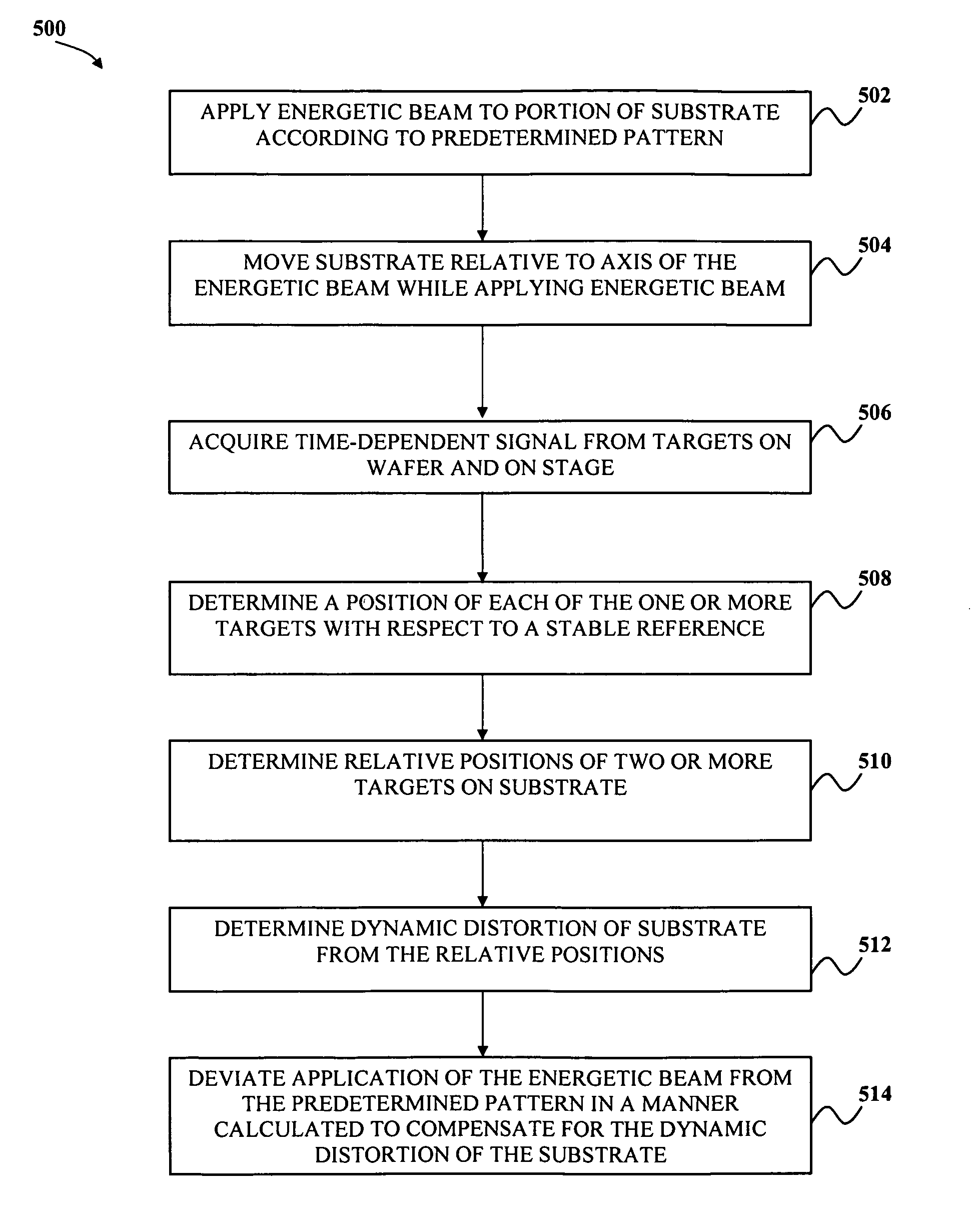
Dynamic tracking of wafer motion and distortion during lithography
a technology of dynamic tracking and lithography, applied in the direction of instruments, printers, therapy, etc., can solve the problems of field-by-field alignment not taking into account the distortions occurring during the movement of the wafer, and the wafer on the stage may move with resp
- Summary
- Abstract
- Description
- Claims
- Application Information
AI Technical Summary
Benefits of technology
Problems solved by technology
Method used
Image

Examples
Embodiment Construction
[0020]Although the following detailed description contains many specific details for the purposes of illustration, anyone of ordinary skill in the art will appreciate that many variations and alterations to the following details are within the scope of the invention. Accordingly, the exemplary embodiments of the invention described below are set forth without any loss of generality to, and without imposing limitations upon, the claimed invention.
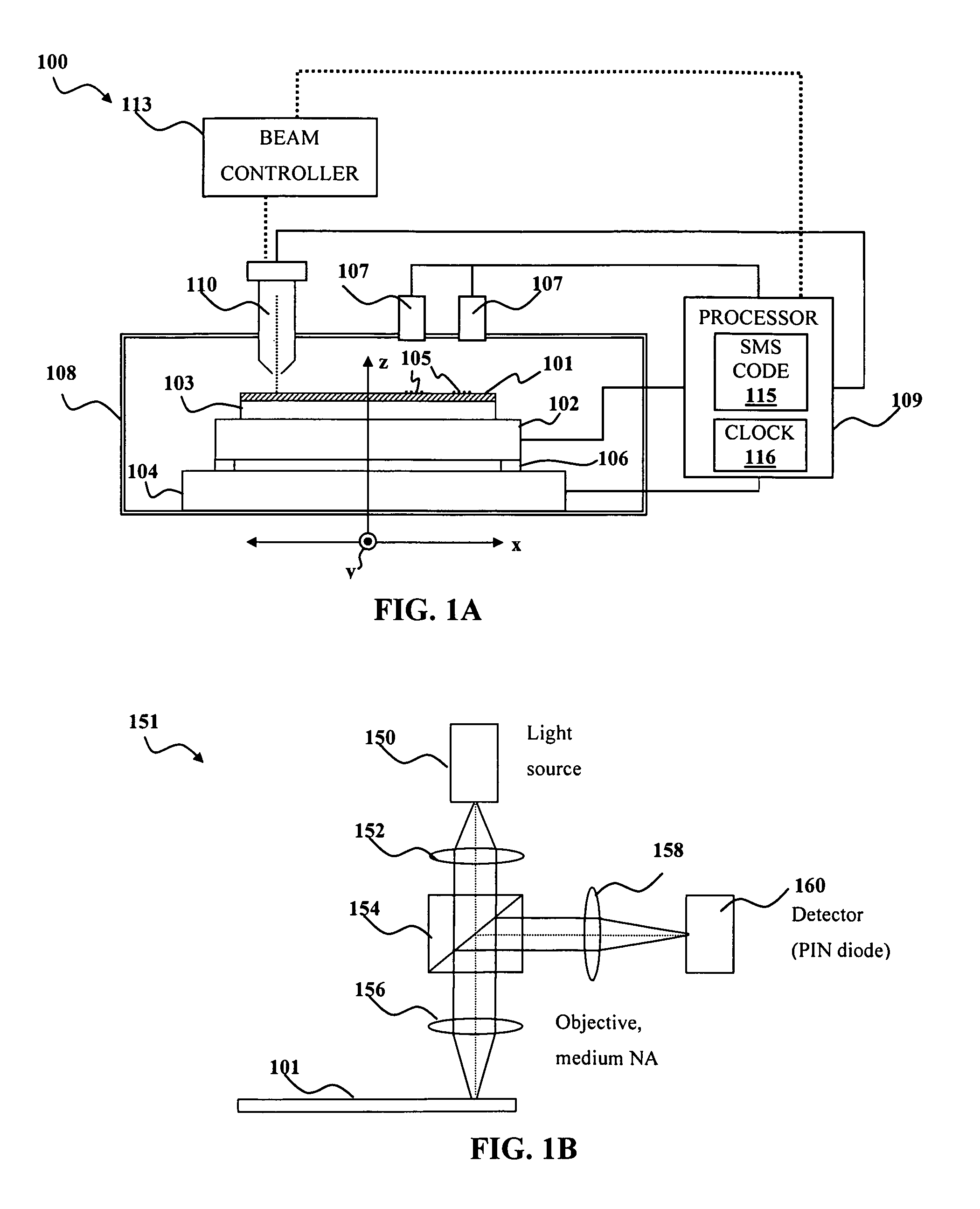
[0021]A recent development in lithography is the use of high-speed electron beam writing. Examples of high-speed electron beam lithography systems and methods are described, e.g., in commonly-assigned U.S. patent application Ser. No. 11 / 670,896 to Marek Zywno and Noah Bareket, which was filed on Feb. 2, 2007, the disclosures of which are incorporated herein by reference. In such systems, multiple wafers may be spun by a rotating stage relative to an electron beam. The rotary stage translates with respect to the beam as it spins. The result i...
PUM
 Abstract
Description
Claims
Application Information