Interconnect layer of a modularly designed analog integrated circuit

a modular design and integrated circuit technology, applied in the field of integrated circuit design and layout, can solve the problems of parasitic resistance, capacitance and inductance, unnecessarily waste of space in the assembly of the integrated circuit in a package with wire bonds, etc., and achieve the effect of faster design and efficient implementation

Active Publication Date: 2011-03-08
ACTIVE SEMI
View PDF10 Cites 43 Cited by
  • Summary
  • Abstract
  • Description
  • Claims
  • Application Information

AI Technical Summary

Benefits of technology

[0014]In one such alternative embodiment, a top metal redistribution layer re-routes the I / O terminals to bond pads located at the perimeter of the combined modular tiles to accommodate wire bonding to package leads of an IC package. In one embodiment, the bond pads are located outside the lateral boundary of the combined modular tiles. In another embodiment, the bond pads are located at the perimeter of the active area defined by the combined modular tiles. The bond pads over the combined modular tiles are known as bond pads over active area (BOAC). Redistributing the I / O terminals to enable wire-bond packaging allows PMICs to be designed quicker and implemented more efficiently even if parasitics are not reduced by adopting chip-scale packaging.

Problems solved by technology

Unfortunately, the prior art suffers from parasitic resistance, capacitance and inductance (parasitics) associated with the internal integrated circuit interconnections from the functional blocks in the core to the I / O pads, and from the parasitics related to the wire bonds and package pins, in the case of traditional wire bond type packages.
Furthermore, the assembly of the integrated circuit in a package with wire bonds and pins unnecessarily wastes space, which is critical in certain space limited applications.
In the case of flip-chip CSP, the prior art also suffers from redistribution layer (RDL) routing parasitics.
Furthermore, prior art approaches lack the ability easily to be reconfigured or rearranged to create new products or derivative products.
In the former case, the die size and cost is not optimal, while in the latter case, the integrated circuit re-layout time requires additional research and development time and resources, which are very expensive.
In both cases, adding or subtracting circuitry to modify existing products or to create new ones, adds risk and cost.

Method used


Image

  • Interconnect layer of a modularly designed analog integrated circuit
  • Interconnect layer of a modularly designed analog integrated circuit
  • Interconnect layer of a modularly designed analog integrated circuit

Examples


Embodiment Construction

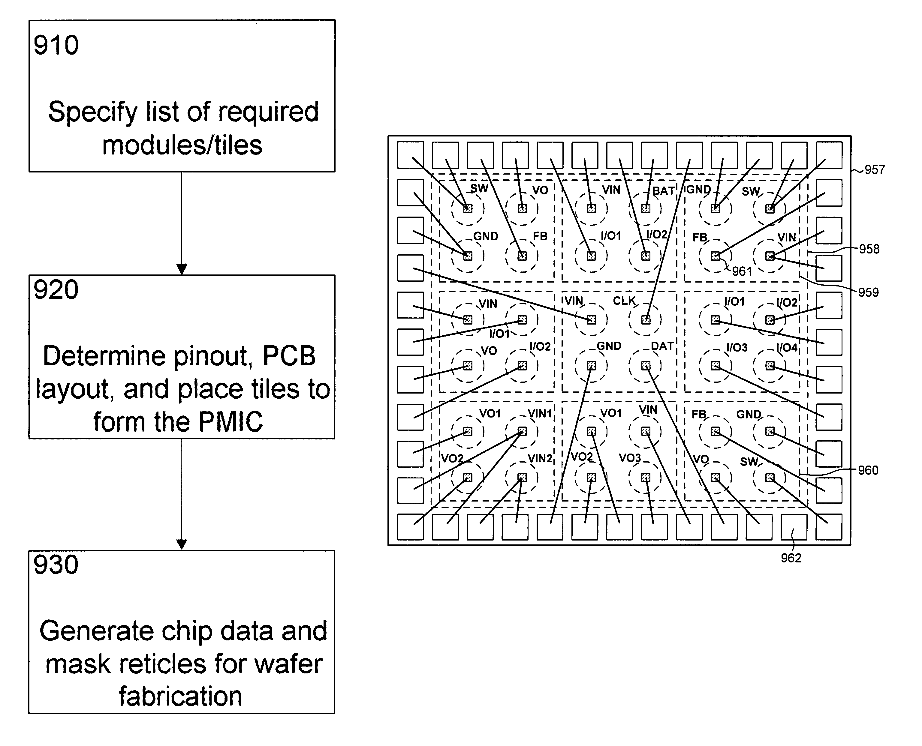
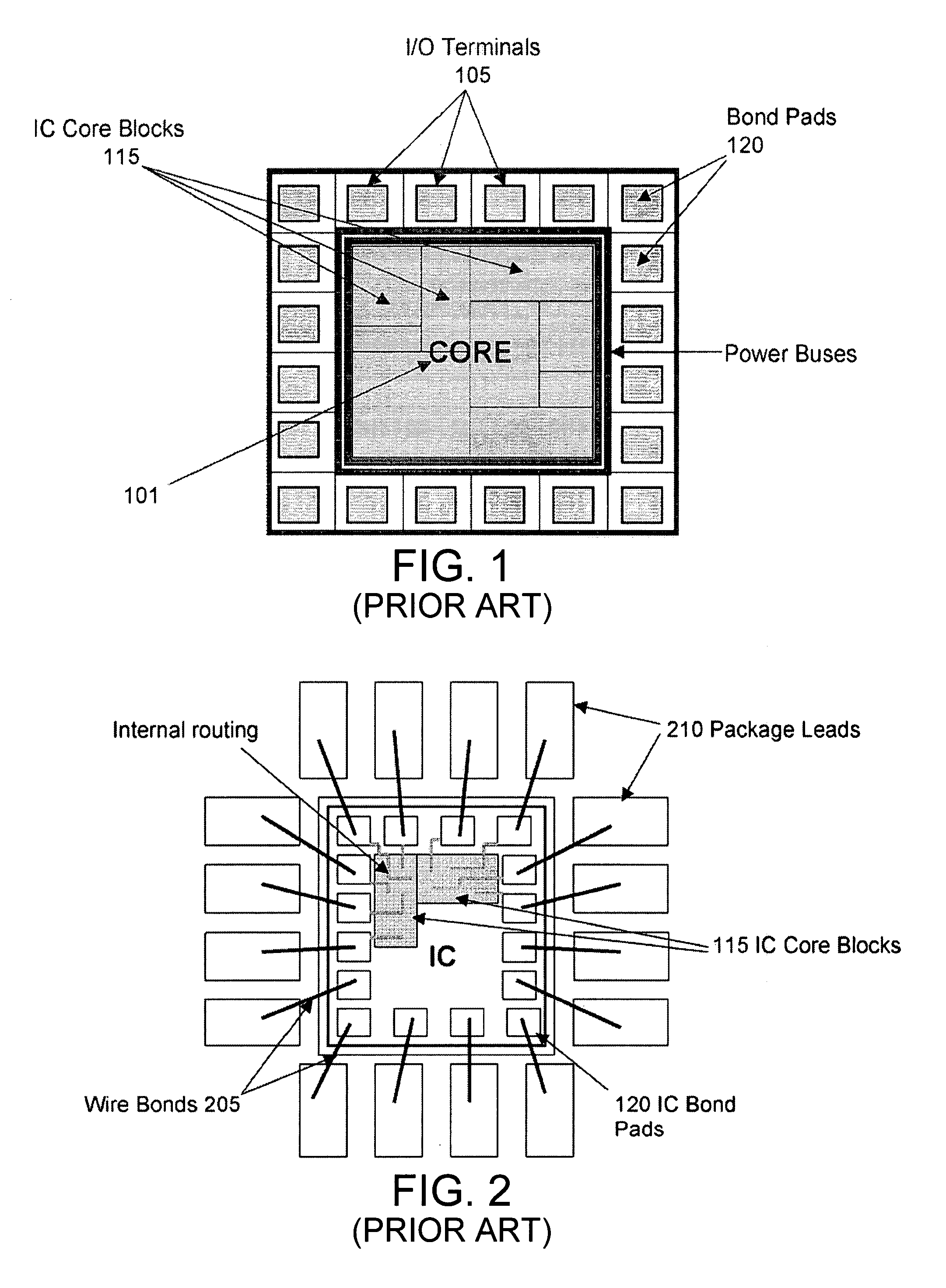
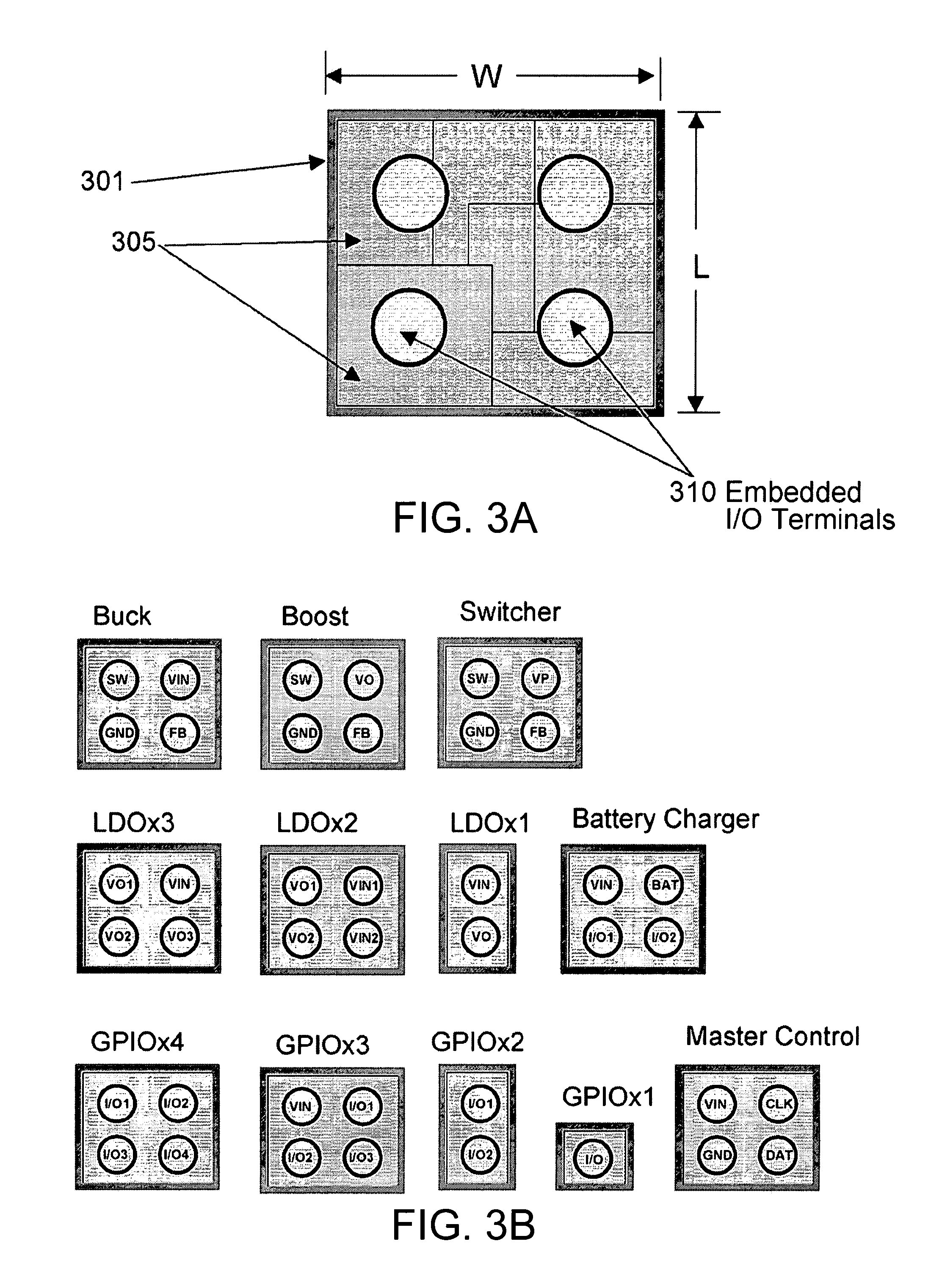
[0033]Embodiments of the invention are discussed below with reference to the figures. However, those skilled in the art will readily appreciate that the detailed description given herein with respect to these figures is for explanatory purposes as the invention extends beyond these limited embodiments. For example, it should be appreciated that those skilled in the art will, in light of the teachings of the present invention, recognize a multiplicity of alternate and suitable approaches, depending upon the needs of the particular application, to implement the functionality of any given detail described herein, beyond the particular implementation choices in the following embodiments described and shown. That is, there are numerous modifications and variations of the invention that are too numerous to be listed but that all fit within the scope of the invention.

[0034]The present invention will now be described in detail with reference to embodiments thereof as illustrated in the acco...


PUM


Abstract

A method of constructing an integrated circuit involves selecting modular tiles and then generating a functional circuit layout using the tiles. Modular tiles that perform predetermined functions and that have approximately the same length and width dimensions are selected from a library of validated tiles. The tiles have input-output terminals embedded in their upper active layers. A functional circuit layout for the integrated circuit is generated using the tiles. In many implementations, the physical layout of the integrated circuit does not include the step of routing. Then an interconnect layer is added over the functional circuitry of the tiles and connects the input-output terminals to bond pads located at the perimeter of the functional circuit layout. Chip data corresponding to the functional circuit layout is generated, and then mask reticles corresponding to the chip data are generated. The integrated circuit is formed on a wafer based on the mask reticles.

Description

CROSS REFERENCE TO RELATED APPLICATION[0001]This application is a continuation-in-part of, and claims priority under 35 U.S.C. §120 from, nonprovisional U.S. patent application Ser. No. 11 / 544,876, entitled “Method and System for the Modular Design and Layout of Integrated Circuits,” filed on Oct. 7, 2006 now U.S. Pat. No. 7,581,198, the subject matter of which is incorporated herein by reference.TECHNICAL FIELD[0002]The present invention relates to the design and layout of integrated circuits (ICs). More specifically, the invention relates to a modular partition approach used to create extremely versatile high performance, application specific ICs in the shortest possible time frame.BACKGROUND INFORMATION[0003]An example of a traditional IC comprised of a core circuit and input / output (I / O) terminals is illustrated by way of example in FIG. 1. The core circuit is typically comprised of several functional blocks. For example, in a multi-output power management integrated circuit (PM...

Claims


Application Information

Patent Timeline
Patent Type & Authority Patents(United States)
IPC IPC(8): G06F17/50
CPCG06F17/5072H01L2224/49171H01L2924/0002H01L2924/00G06F30/392
Inventor HUYNH, STEVENKUNST, DAVID
Owner ACTIVE SEMI
Why Eureka
Try Eureka