Electrophotographic photoreceptor, and image forming apparatus and process cartridge using the same

a technology of photoreceptor and image forming apparatus, which is applied in the direction of electrographic process, instrumentation, corona discharge, etc., can solve the problems of image blurring, accelerated abrasion of the photoreceptor, and gradual deterioration of the surface of the photoreceptor

Inactive Publication Date: 2011-03-15
FUJIFILM BUSINESS INNOVATION CORP
View PDF10 Cites 4 Cited by
  • Summary
  • Abstract
  • Description
  • Claims
  • Application Information

AI Technical Summary

Benefits of technology

[0026]Thus, in the exemplary embodiment of the invention, since the photoreceptor has a structure in which the intermediate layer having a thickness within the above-mentioned range and the surface layer are disposed in this order on the photosensitive layer and the refractive indices satisfy Inequality (1), the variation in the total amount of the reflected light from the photoreceptor is substantially equal to the variation in the amount of reflected light from a photoreceptor without an intermediate layer and a surface layer. Therefore, the variation in the amount of the light that has been irradiated to the photoreceptor and incident to the photosensitive layer, resulting from unevenness in the thickness of the surface layer, is suppressed, whereby generation of unevenness in image density is suppressed.
[0042]As a result, an electrophotographic organic photoreceptor is provided which has excellent surface mechanical durability, oxidation resistance, and high sensitivity, and with which image defects due to deposition of discharge products are suppressed and quality (e.g., excellent uniformity of outputted images) is easily maintained at high level over time.
[0069]Moreover, the surface layer 3 of the exemplary embodiment of the invention may contain a Group 13 element and at least one of nitrogen or oxygen. When the surface layer 3 contains such elements, the surface layer may have high hardness and excellent transparency As in the case of the intermediate layer 5, incorporation of oxygen into the surface layer 3 may provide excellent oxidation resistance when exposed to oxygen in the air or to an oxidative atmosphere, and may cause less change in physical properties over time.
[0026]Thus, in the exemplary embodiment of the invention, since the photoreceptor has a structure in which the intermediate layer having a thickness within the above-mentioned range and the surface layer are disposed in this order on the photosensitive layer and the refractive indices satisfy Inequality (1), the variation in the total amount of the reflected light from the photoreceptor is substantially equal to the variation in the amount of reflected light from a photoreceptor without an intermediate layer and a surface layer. Therefore, the variation in the amount of the light that has been irradiated to the photoreceptor and incident to the photosensitive layer, resulting from unevenness in the thickness of the surface layer, is suppressed, whereby generation of unevenness in image density is suppressed.
[0066]When the intermediate layer 5 formed is an insulative layer, the thickness of the intermediate layer may be determined in consideration of a residual potential. When the intermediate layer 5 is a semiconductive layer, the volume resistivity thereof may be from 10+8 Ωcm to 10+13 Ωcm in view of not inhibiting latent image formation.
[0024]Specifically, when the photoreceptor has a structure in which a surface layer having a refractive index higher than that of the photosensitive layer is formed on the photosensitive layer without an intermediate layer therebetween, interference between the reflected light from the photosensitive layer and the reflected light from the surface layer is increased, and becomes large. Therefore, intensity variation of the reflected light from the photoreceptor due to unevenness in the thickness of the intact surface layer and / or unevenness in the layer thickness caused by abrasion is increased, and, resultantly, image unevenness easily occurs.
[0032]Since the surface layer and the intermediate layer each contain an oxide or nitride of a Group 13 element, the photoreceptor surface itself may be difficult to oxidize in an oxidizing atmosphere containing, for example, ozone or a nitrogen oxide generated by a charger in an image-forming apparatus. Therefore, deterioration of the photoreceptor due to oxidation may be prevented. Moreover, due to excellent mechanical durability and oxidation resistance of the photoreceptor, the properties required for a photoreceptor may be easily maintained at a high level over a long period of time. The surface of the photoreceptor, which is rubbed by a cleaning blade or the like, may have excellent abrasion resistance, and may be less likely to be damaged. Consequently, sufficient sensitivity may be easily obtained.
[0024]Specifically, when the photoreceptor has a structure in which a surface layer having a refractive index higher than that of the photosensitive layer is formed on the photosensitive layer without an intermediate layer therebetween, interference between the reflected light from the photosensitive layer and the reflected light from the surface layer is increased, and becomes large. Therefore, intensity variation of the reflected light from the photoreceptor due to unevenness in the thickness of the intact surface layer and / or unevenness in the layer thickness caused by abrasion is increased, and, resultantly, image unevenness easily occurs.
[0024]Specifically, when the photoreceptor has a structure in which a surface layer having a refractive index higher than that of the photosensitive layer is formed on the photosensitive layer without an intermediate layer therebetween, interference between the reflected light from the photosensitive layer and the reflected light from the surface layer is increased, and becomes large. Therefore, intensity variation of the reflected light from the photoreceptor due to unevenness in the thickness of the intact surface layer and / or unevenness in the layer thickness caused by abrasion is increased, and, resultantly, image unevenness easily occurs.
[0042]As a result, an electrophotographic organic photoreceptor is provided which has excellent surface mechanical durability, oxidation resistance, and high sensitivity, and with which image defects due to deposition of discharge products are suppressed and quality (e.g., excellent uniformity of outputted images) is easily maintained at high level over time.

Problems solved by technology

For example, in non-contact charging, discharge products deposit on the photoreceptor, which cause image blurring or the like.
However, in such a system, a surface of the photoreceptor is deteriorated gradually due to abrasion.
However, the contact charging may accelerate abrasion of the photoreceptor as well.
Because of these issues, prolongation of the lifetime of electrophotographic photoreceptors has been required.

Method used


Image

  • Electrophotographic photoreceptor, and image forming apparatus and process cartridge using the same
  • Electrophotographic photoreceptor, and image forming apparatus and process cartridge using the same
  • Electrophotographic photoreceptor, and image forming apparatus and process cartridge using the same

Examples


example 1

Preparation of Electrophotographic Photoreceptor

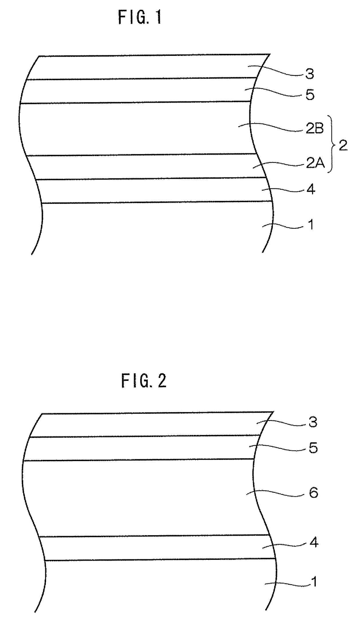
[0263]According to the following procedure, an undercoat layer, a charge generation layer, and a charge transport layer are formed on a substrate Al in this order to give an organic photoreceptor.

[0264]Formation of Undercoat Layer

[0265]One hundred parts by weight of zinc oxide (average particle diameter: 70 nm) are mixed with 500 parts by weight of tetrahydrofuran under stirring. To the mixture, 1.25 parts by weight of a silane coupling agent (trade name: KBM603, manufactured by Shin-Etsu Chemical Co., Ltd.) are added and stirred for 2 hours. Subsequently, baking is conducted to obtain a zinc oxide pigment whose surface is treated with the silane-coupling agent.

[0266]60 parts by weight of the surface-treated zinc oxide, 0.6 part by weight of alizarin, 13.5 parts by weight of a curing agent (blocked isocyanate, trade name: SUMIDUR 3175, manufactured by Sumika Bayer Urethane Co., Ltd.), and 15 parts by weight of a butyral resin (trade na...

example 9 and example 10

Formation of Surface Layer

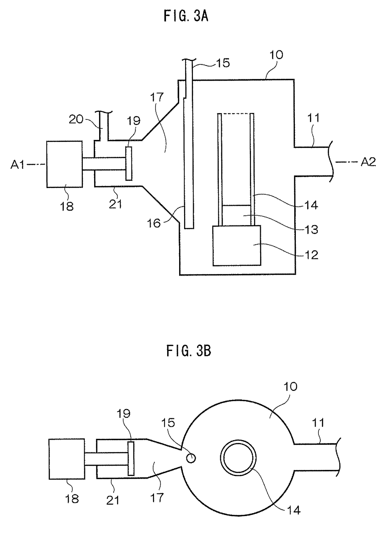
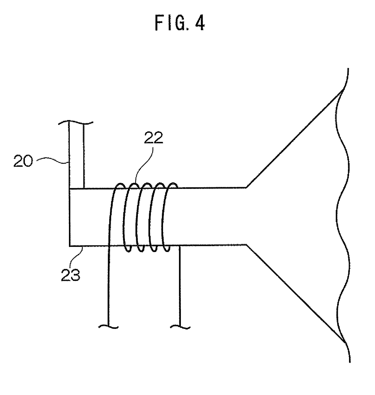
[0282]Subsequent to the formation of the intermediate layer, He gas, hydrogen gas, and oxygen gas diluted to 4% by He gas are mixed in a mixing device (not shown in drawings), and the mixture gas is introduced from a gas supply tube 20 towards an flat plate electrode 19 having a length of 350 mm at a flow rate of about 352 sccm (He gas: 150 sccm, hydrogen: 200 sccm, oxygen: 2 sccm). Electric discharge is performed from the flat plate electrode 19 by setting an output of 13.65 MHz radio frequency wave to 80 W with matching by a tuner, using a high-frequency power supply unit 18 and a matching circuit (not shown in the drawings). The reflected wave at discharge is 0 W.

[0283]Subsequently, trimethyl gallium gas is introduced from a shower nozzle 16 into a film-forming chamber 10 through a gas inlet tube 15 at a trimethyl gallium gas flow rate of 1.0 sccm. At this time, the reaction pressure in the film-forming chamber 10 determined by a Baratron vacuum gauge is...

examples 2 to 10

[0315]In Example 2 to 6, photoreceptors A2 to A6 in which an intermediate layer and an surface layer are formed on the non-coated photoreceptor in this order are prepared in the same manner as in Example 1 except that the types and composition ratio of the contained elements and the film formation time are changed as shown in Table 1. The photoreceptors A2 to A6 thus obtained are evaluated in the same manner as in Example 1. The results of the evaluation are shown in Table 1. Further, in Examples 7 to 10, photoreceptors A7 to A10 in which an intermediate layer and an surface layer are formed on the non-coated photoreceptor in this order are prepared in the same manner as in Example 1 except that the types and composition ratio of the contained elements and the film formation time are changed as shown in Table 1. The intermediate layers of the photoreceptors A7 to A10 contain Ga, N, and O. The photoreceptors A7 to A10 thus obtained are evaluated in the same manner as in Example 1, an...


PUM

PropertyMeasurementUnit
thicknessaaaaaaaaaa
refractive index n2aaaaaaaaaa

Abstract

An electrophotographic photoreceptor includes a conductive substrate, and a photosensitive layer, an intermediate layer having a thickness of 2 nm to 70 nm, and a surface layer, which are disposed in this order on the conductive substrate. The refractive index n1 of the photosensitive layer, the refractive index n2 of the intermediate layer, and the refractive index n3 of the surface layer satisfy an inequality, n2>n3>n1.

Description

CROSS-REFERENCE TO RELATED APPLICATION[0001]This application is based on and claims priority under 35 USC 119 from Japanese Patent Application No. 2008-098477 filed on Apr. 4, 2008.BACKGROUND[0002]1. Technical Field[0003]The invention relates to an electrophotographic photoreceptor for use in, for example, a copying machine that forms an image by an electrophotographic method, and a process cartridge and an image-forming apparatus using the electrophotographic photoreceptor.[0004]2. Related Art[0005]In recent years, the electrophotographic method has been used widely, for example, in copying machines and printers. An electrophotographic photoreceptor for use in image-forming apparatuses utilizing the electrophotographic method (hereinafter, sometimes referred to as a “photoreceptor”) comes into contact with various materials and is exposed to various stresses in the apparatus and thus deteriorates gradually. On the other hand, digitalization and colorization of image-forming apparat...

Claims


Application Information

Patent Timeline
Patent Type & Authority Patents(United States)
IPC IPC(8): G03G5/06
CPCG03G5/0436G03G5/0525G03G5/0564G03G5/0614G03G5/0696G03G5/144G03G5/14704G03G5/061443
Inventor YAGI, SHIGERUIWANAGA, TAKESHINISHIKAWA, MASAYUKITORIGOE, NOBUYUKI
Owner FUJIFILM BUSINESS INNOVATION CORP
Why Eureka
Try Eureka