III-nitride light-emitting devices with one or more resonance reflectors and reflective engineered growth templates for such devices, and methods

a technology of resonance reflector and light-emitting device, which is applied in the direction of semiconductor devices, basic electric elements, electrical apparatus, etc., can solve the problems of n-type gan layer side being buried, surface texturing and photonic crystal structure suffering from added complexity, and difficult access from the substrate side for further processing, etc., to achieve easy commercialization, less process intensive, and increase the effect of electrical current injection and current distribution

Active Publication Date: 2011-03-29
LIGHTWAVE PHOTONICS INC
View PDF34 Cites 22 Cited by
  • Summary
  • Abstract
  • Description
  • Claims
  • Application Information

AI Technical Summary

Benefits of technology

[0034]To create a resonant cavity device, the GEMM may be placed at or close to a standing optical wave node to create constructive interference between the light generated by the active region and the reflected light from the GEMM. This enables light to be directed into modes (or a single mode) to increase the amount of light propagating out of the LED. Light generated by optical cavity devices are more directional and spectrally pure compared to standard LEDs.
[0036]Appropriately utilized GEMM layers have a number of advantages over current appropriately utilized device structure components like Distributed Bragg Reflectors (DBRs) or non-epitaxial mirrors.
[0038]Embedding a planar specular GEMM layer within a light emitting device structure, such that optical cavity structures described herein are formed, may not involve material removal such as laser-lift-off or material etching. The steps to create these alternative structures with the GEMM are less process intensive and more easily commercialized compared to other structures described above.
[0039]Additionally, the GEMM layer may be used as a conductive layer to increase electrical current injection and current distribution. Furthermore, the superior current distribution may improve electrostatic discharge reliability.

Problems solved by technology

Surface texturing and photonic crystal structures suffer from added complexity due to extra techniques and processing steps which may include extra layer formation or etching steps.
Because the sapphire substrate is nonconductive and it is preferred to grow the conductive n-type GaN layer side first, the n-type GaN layer side becomes buried and difficult to access from the substrate side for further processing due to the extreme hardness of sapphire.
The alternating material layers often suffer from a lattice mismatch that may lead to increased wafer cracking, poorer crystal quality, reduced yield, lower uniformity, and higher manufacturing cost.
Moreover, DBRs are more electrically resistive, compared to metal or other semiconductor materials, resulting in poor current injection into the device.
Nevertheless, while potentially an improvement over previous DBRs, the device has not adequately solved the manufacturing complexities or conductivity shortcomings inherent in DBR material composition.
While this approach has been shown to function, the process of laser-lift-off and subsequent etching is difficult to commercialize and to obtain high yields.

Method used


Image

  • III-nitride light-emitting devices with one or more resonance reflectors and reflective engineered growth templates for such devices, and methods
  • III-nitride light-emitting devices with one or more resonance reflectors and reflective engineered growth templates for such devices, and methods
  • III-nitride light-emitting devices with one or more resonance reflectors and reflective engineered growth templates for such devices, and methods

Examples


first embodiment

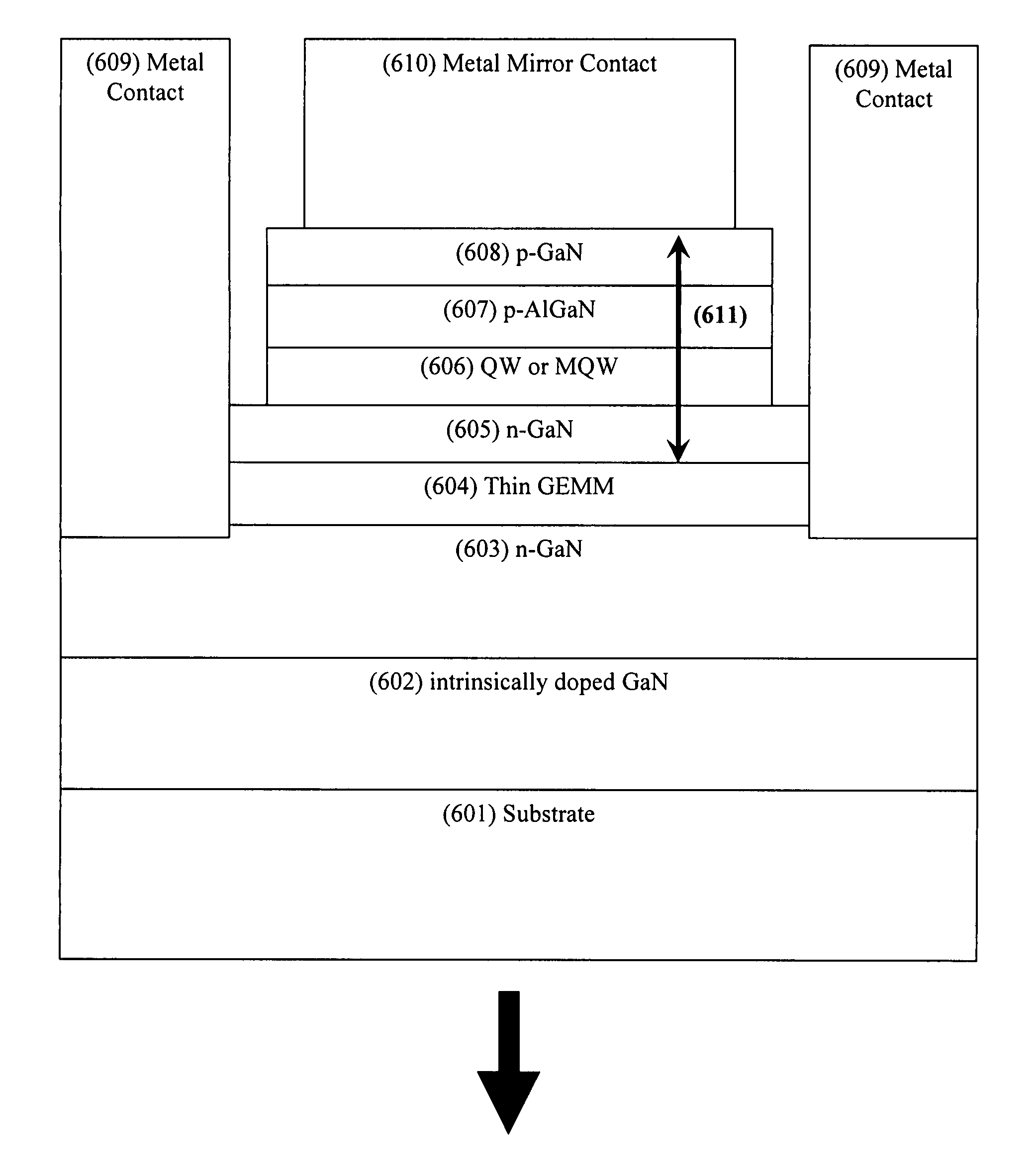
[0095]The structure and band diagram of the first embodiment are shown in FIG. 6 and FIG. 7 respectively.

[0096]The GEMM (604) lends itself to many forms of optical cavity semiconductor light emitters. In the first embodiment the GEMM (604), with its highly reflective bulk properties, may be grown thin such that the GEMM (604) is partially transparent and partially reflective. The first embodiment utilizes a planar III-nitride material growth template comprising of sapphire substrate (601), i-GaN buffer layer (602) and n-GaN layer (603) of device quality so that the crystal quality of the GEMM (604) is planar, specular and of device quality. The GEMM (604) is lattice matched to the n-GaN layer (603) such that the desired thickness may be below the epitaxial critical thickness.

[0097]Once the 2 μm i-GaN buffer (602) and the 2 μm n-GaN (603) layers are grown on a sapphire substrate (601) the GEMM (604) may be grown to a specific thickness (˜20 nm) for the resonant cavity (611) such that...

second embodiment

[0113]The structure and band diagram of the second embodiment are shown in FIG. 8 and FIG. 9 respectively.

[0114]The GEMM (804) lends itself to many forms of optical cavity semiconductor light emitters. In the second embodiment the GEMM (804), with its highly reflective bulk properties, may be grown thick such that the GEMM (804) takes on its bulk reflective properties. The second embodiment utilizes a planar III-nitride material growth template comprising of sapphire substrate (801), i-GaN buffer layer (802) and n-GaN layer (803) of device quality so that the crystal quality of the GEMM (804) is planar, specular and of device quality. The GEMM (804) is lattice matched to the n-GaN layer (803) such that the desired thickness may be below the epitaxial critical thickness.

[0115]Once the 2 μm i-GaN buffer (802) and the 2 μm n-GaN (803) layers are grown on a sapphire substrate (801) the GEMM (804) may be grown to a thickness (≧150 nm) for the resonant cavity (812). Once the GEMM (804) is...

third embodiment

[0129]The structure and band diagram of the third embodiment are shown in FIG. 10 and FIG. 11, respectively.

[0130]The GEMM (1004) lends itself to many forms of optical cavity semiconductor light emitters. In the third embodiment the GEMM (1004), with its highly reflective bulk properties, may be grown thick such that the GEMM (1004) takes on its bulk reflective properties. The third embodiment utilizes a planar III-nitride material growth template comprising of sapphire substrate (1001), i-GaN buffer layer (1002) and n-GaN layer (1003) of device quality so that the crystal quality of the GEMM (1004) is planar, specular and of device quality. The GEMM (1004) is lattice matched to the III-nitride n-GaN layer (1003) such that the desired thickness may be below the epitaxial critical thickness.

[0131]Once the 2 μm i-GaN buffer (1002) and the 2 μm n-GaN (1003) layers are grown on a sapphire substrate (1001) the GEMM (1004) may be grown to a thickness (≧150 nm) for the surface roughened as...


PUM

PropertyMeasurementUnit
thickaaaaaaaaaa
thicknessaaaaaaaaaa
extraction efficiencyaaaaaaaaaa

Abstract

A light emitter includes a first mirror that is an epitaxially grown metal mirror, a second mirror, and an active region that is epitaxially grown such that the active region is positioned at or close to, at least, one antinode between the first mirror and the second mirror.

Description

[0001]This application claims the benefit under 35 U.S.C. Section 119(e) of the following U.S. provisional patent applications:[0002]U.S. Provisional Patent Application Ser. No. 60 / 835,934, filed on Aug. 6, 2006, by R. J. Jorgenson, entitled “III-NITRIDE LIGHT-EMITTING DEVICES WITH ONE OR MORE RESONANCE REFLECTORS AND REFLECTIVE ENGINEERED GROWTH TEMPLATES FOR SUCH DEVICES, AND METHODS.”[0003]U.S. Provisional Patent Application Ser. No. 60 / 821,588, filed on Aug. 7, 2006, by R. J. Jorgenson, entitled “III-NITRIDE LIGHT-EMITTING DEVICES WITH ONE OR MORE RESONANCE REFLECTORS AND REFLECTIVE ENGINEERED GROWTH TEMPLATES FOR SUCH DEVICES, AND METHODS.”[0004]Both of the provisional applications identified above are incorporated by reference herein.BACKGROUND[0005]1. Field of Invention[0006]The invention is related to semiconductor light emitters.[0007]2. Description of Related Art[0008]Throughout this application, references are cited. The respective disclosure of each of these references i...

Claims


Application Information

Patent Timeline
Patent Type & Authority Patents(United States)
IPC IPC(8): H01L29/22
CPCH01L33/105H01L33/32H01L33/60H01L33/465H01L33/405
Inventor JORGENSON, ROBBIE J.
Owner LIGHTWAVE PHOTONICS INC
Why Eureka
Try Eureka