Planar microshells for vacuum encapsulated devices and damascene method of manufacture

a technology of vacuum encapsulation and microelectronic devices, applied in the direction of microstructural systems, instruments, acceleration measurement using interia forces, etc., can solve the problems of affecting the cost and functionality of mems or microelectronic devices, affecting the freedom of movement during operation, and many devices not working properly

Active Publication Date: 2011-04-12
SEMICON MFG INT (SHANGHAI) CORP
View PDF53 Cites 122 Cited by
  • Summary
  • Abstract
  • Description
  • Claims
  • Application Information

AI Technical Summary

Problems solved by technology

Many devices, particularly MEMS do not function properly when embedded in a completely solid environment.
Freedom to move during operation would be lost if these elements were simply left embedded in a solid film deposited over the substrate as is commonly done in the microelectronics industry.
The type of package employed for such a MEMS or microelectronic device greatly affects their cost and functionality.
This type of packaging is not wafer-level and is limited to stand-alone (discrete) devices, and therefore is expensive.
Fabrication of microcap packages of the type shown is frequently more expensive than the fabrication of the devices they protect.
Fabrication and alignment of second substrate 105 is costly and, as shown, seal ring 110 requires a significant amount of die area, thereby increasing the cost by limiting the minimum dimension of the package.
Thus, the microcap package limits the scaling of the packaged device, accounts for a large percentage of the packaged device cost and limits wafer-level integration of devices requiring a fluidic environment with those that do not.
However, one issue with the conventional microshells is that the pressure inside the microshell is not controllable as in the microcap bonding process.
Sealing the microshell with a silicon dioxide process typically limits the level of vacuum that can be achieved within the microshell and can result in contamination on the encapsulated device.
Furthermore, conventional microshells are not as robust as bonded microcap packages and so, as the chamber size is inc

Method used


Image

  • Planar microshells for vacuum encapsulated devices and damascene method of manufacture
  • Planar microshells for vacuum encapsulated devices and damascene method of manufacture
  • Planar microshells for vacuum encapsulated devices and damascene method of manufacture

Examples


Embodiment Construction

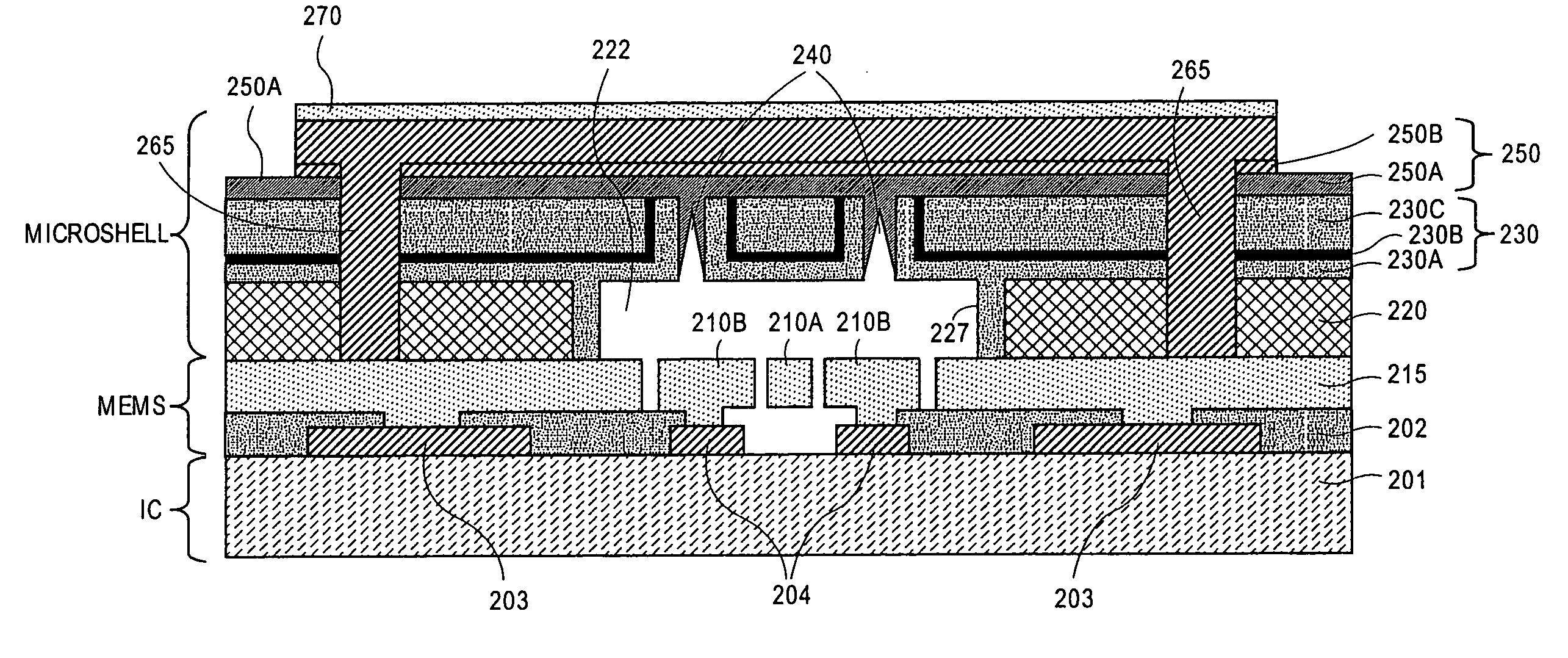
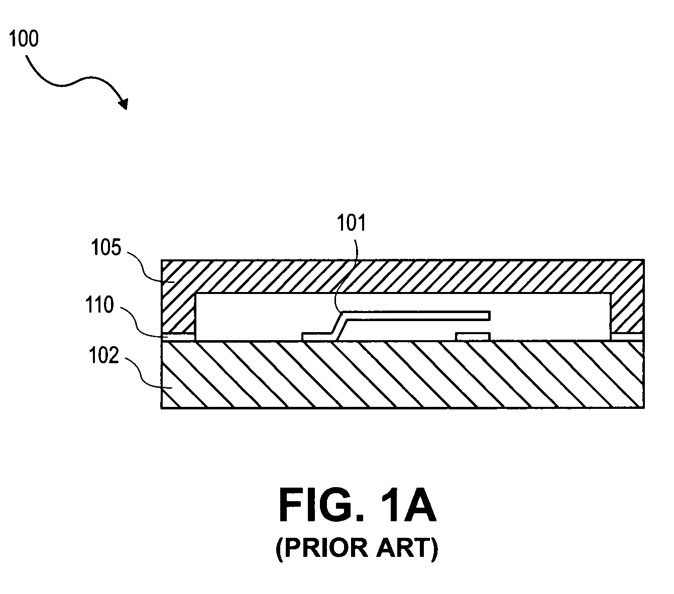
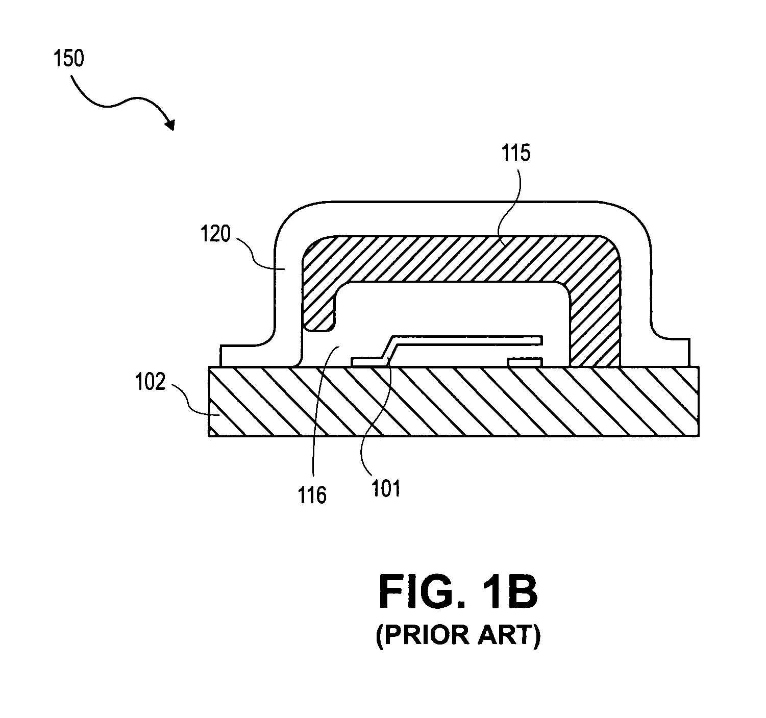
In various embodiments, microshells are described herein with reference to figures. However, certain embodiments may be practiced without one or more of these specific details, or in combination with other known methods and materials. In the following description, numerous specific details are set forth, such as specific materials, dimensions and processes, etc., in order to provide a thorough understanding of the present invention. In other instances, well-known manufacturing processes and techniques have not been described in particular detail in order to not unnecessarily obscure the present invention. Reference throughout this specification to “an embodiment” means that a particular feature, structure, material, or characteristic described in connection with the embodiment is included in at least one embodiment of the invention. Thus, the appearances of the phrase “in an embodiment” in various places throughout this specification are not necessarily referring to the same embodim...


PUM


Abstract

Low temperature, multi-layered, planar microshells for encapsulation of devices such as MEMS and microelectronics. The microshells include a planar perforated pre-sealing layer, below which a non-planar sacrificial layer is accessed, and a sealing layer to close the perforation in the pre-sealing layer after the sacrificial material is removed. In an embodiment, the pre-sealing layer has perforations formed with a damascene process to be self-aligned to the chamber below the microshell. The sealing layer may include a nonhermetic layer to physically occlude the perforation and a hermetic layer over the nonhermetic occluding layer to seal the perforation. In a particular embodiment, the hermetic layer is a metal which is electrically coupled to a conductive layer adjacent to the microshell to electrically ground the microshell.

Description

CROSS-REFERENCE TO RELATED APPLICATIONSThis patent application is related to the following U.S. patent applications:Non-provisional patent application entitled “Thin Film Microshells Incorporating a Getter Layer” having Ser. No. 11 / 716,422, filed the same day as this patent application.Non-provisional patent application entitled “Low Stress Thin Film Microshell” having Ser. No. 11 / 716,233, filed the same day as this patent application.Non-provisional patent application entitled “Thin Film Microshell for Multi-level Vacuum Cavities” having Ser. No. 11 / 716,156, filed the same day as this patent application.BACKGROUND1. FieldThe present invention relates to the field of manufacturing of microelectronic devices and microelectromechanical systems (MEMS), and more particularly to the formation of microshells to encapsulate such devices on a substrate.2. Discussion of Related ArtThe term “MEMS” generally refers to an apparatus incorporating some mechanical structure having a dimensional sc...

Claims


Application Information

Patent Timeline
IPC IPC(8): H01L29/84
CPCB81C1/00333B81C2203/0145B81C2203/0136B81C2203/0771B81C2203/0721B81B7/02B81C1/00246B81C1/00293B81C2203/0735
Inventor QUEVY, EMMANUEL P.MONADGEMI, PEZHMANHOWE, ROGER T.
Owner SEMICON MFG INT (SHANGHAI) CORP
Why Eureka
Try Eureka