Method and apparatus for electroplating

a technology of electroplating and surface treatment, which is applied in the direction of electrolysis components, electric circuits, manufacturing tools, etc., can solve the problems of extreme terminal effect situation, non-uniform thickness distribution of plating, and significant limitations of approaches related to physical properties of materials and processes, so as to improve plating uniformity

Active Publication Date: 2010-02-11
NOVELLUS SYSTEMS
View PDF101 Cites 173 Cited by
  • Summary
  • Abstract
  • Description
  • Claims
  • Application Information

AI Technical Summary

Benefits of technology

[0015]These needs are herein addressed, in one aspect, by providing an electroplating apparatus and a method for uniform electroplating that make use of an ionically resistive element having electrolyte-permeable 1-D through-holes, where the element resides in close proximity of the wafer substrate. The ionically resistive ionically permeable element described herein substantially improves plating uniformity on thin resistive seed layers. It is particularly useful when employed in combination with a second (thief) cathode confi...

Problems solved by technology

These films present the engineer with an extreme terminal effect situation.
Without appropriate means of resistance and voltage compensation, this large edge-to-center voltage drop could lead to an extremely non-uniform plating thickness distribution, primarily characterized by thicker plating at the wafer edge.
These approaches have significant limitations related to the physical properties of the materials and the processes.
Also, because the conductivity of a plating bath is tied to its ionic concentration and pH, decreasing the conductivity directly and negatively impacts the rate of plating and morphology of the plated material.
In general, entry of a wafer carrying a thin seed layer into electrolyte can lead to a number of serious performance and feature filling issues if entry is not properly controlled (see for example, U.S. Pat. No. 6,949,065, which is herein inco...

Method used


Image

  • Method and apparatus for electroplating
  • Method and apparatus for electroplating
  • Method and apparatus for electroplating

Examples


Embodiment Construction

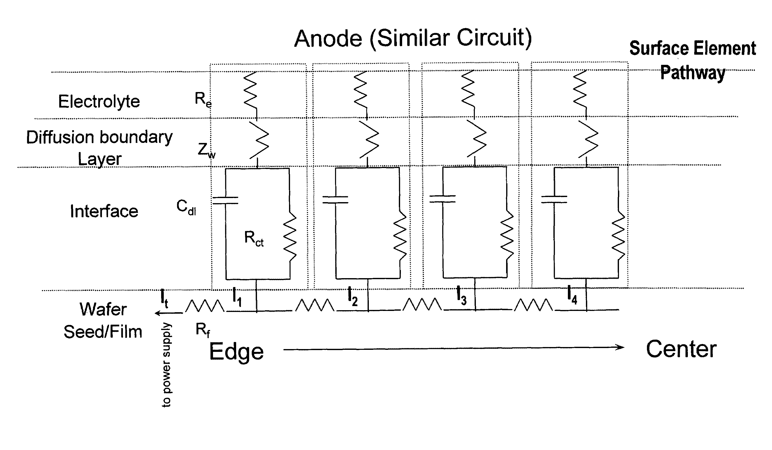
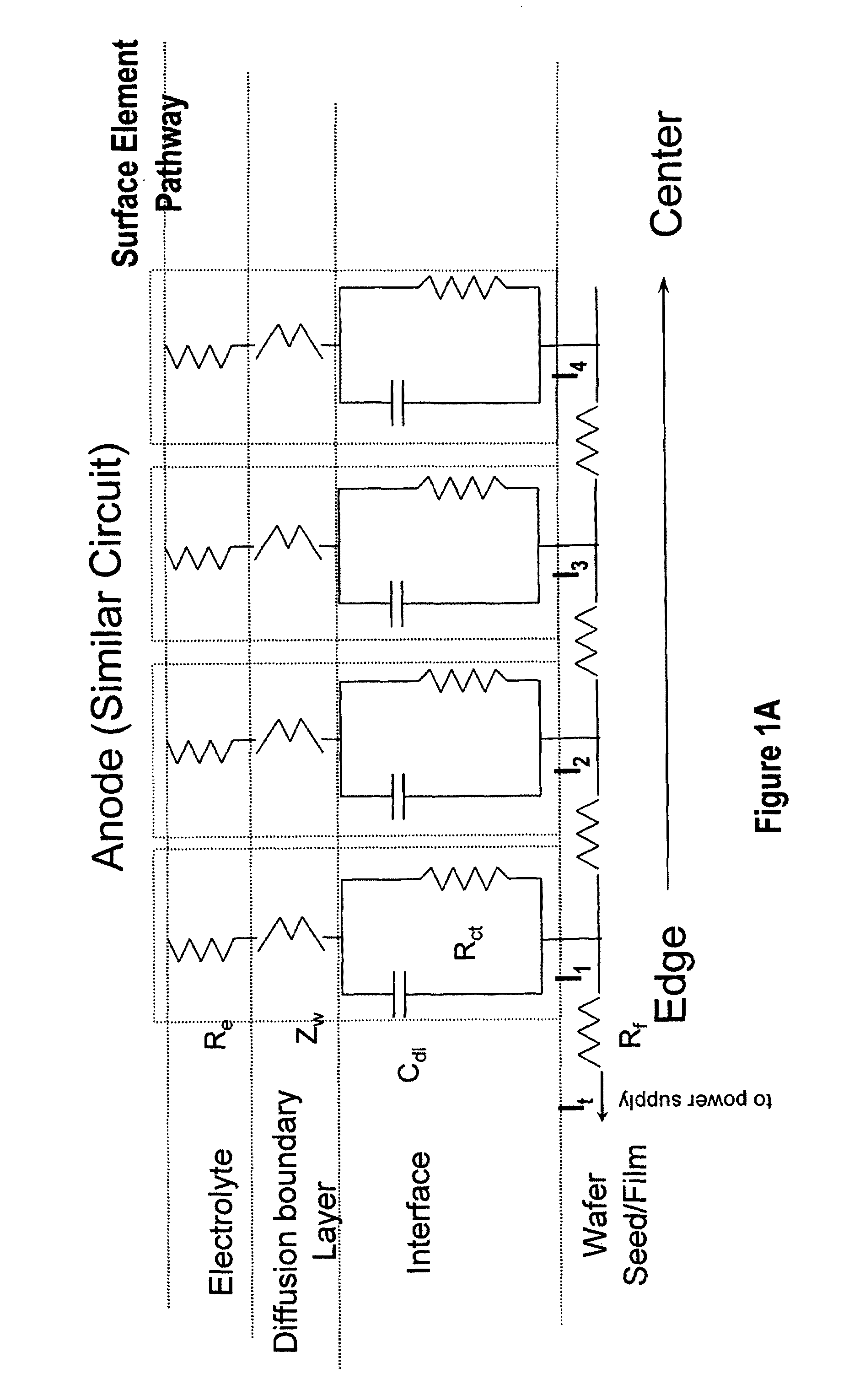
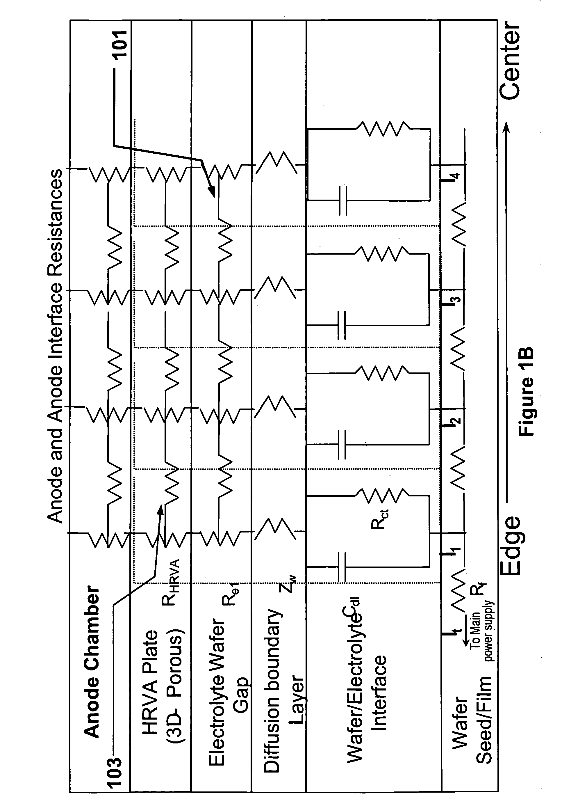
[0054]The present invention pertains to methods and apparatus for electroplating a substantially uniform layer of a metal onto a work piece having a seed layer thereon. This invention mitigates or eliminates the terminal problem by placing an ionically resistive element having a large number of isolated and unconnected ionically permeable through-holes (e.g., a resistive disc having multiple perforations allowing for passage of ions) in close proximity to the work piece, thereby dominating or “swamping” the overall system's resistance. The resistive element thus approximates a constant current source. By keeping the work piece close to the resistive element surface, the ionic resistance from the top of the element to the surface is much less than the ionic path resistance from the top of the element to the work piece edge, substantially compensating for the sheet resistance in the thin metal film and directing a significant amount of current over the center of the work piece. The im...


PUM

PropertyMeasurementUnit
Lengthaaaaaaaaaa
Timeaaaaaaaaaa
Thicknessaaaaaaaaaa

Abstract

An apparatus for electroplating a layer of metal on the surface of a wafer includes an ionically resistive ionically permeable element located in close proximity of the wafer (preferably within 5 mm of the wafer surface) which serves to modulate ionic current at the wafer surface, and a second cathode configured to divert a portion of current from the wafer surface. The ionically resistive ionically permeable element in a preferred embodiment is a disk made of a resistive material having a plurality of perforations formed therein, such that perforations do not form communicating channels within the body of the disk. The provided configuration effectively redistributes ionic current in the plating system allowing plating of uniform metal layers and mitigating the terminal effect.

Description

CROSS-REFERENCE TO RELATED APPLICATIONS[0001]This application is a continuation-in part of U.S. application Ser. No. 11 / 506,054 titled METHOD AND APPARATUS FOR ELECTROPLATING INCLUDING A REMOTELY POSITIONED SECOND CATHODE filed Aug. 16, 2006 naming Reid et al. as inventors, which is herein incorporated by reference in its entirety and for all purposes.FIELD OF THE INVENTION[0002]The present invention relates generally to a method and apparatus for treating the surface of a substrate and more particularly to a method and apparatus for electroplating a layer on a semiconductor wafer. It is particularly useful for electroplating copper in Damascene and dual Damascene integrated circuit fabrication methods.BACKGROUND OF THE INVENTION[0003]The transition from aluminum to copper in integrated circuit (IC) fabrication required a change in process “architecture” (to damascene and dual-damascene) as well as a whole new set of process technologies. One process step used in producing copper da...

Claims


Application Information

Patent Timeline
IPC IPC(8): C25D3/00C25D17/00
CPCC25D21/12H01L21/2885H01L21/76873C25D17/007C25D7/123C25D17/001C25D17/008
Inventor REID, JONATHANBUCKALEW, BRYANHE, ZHIANPARK, SEYANGVARADARAJAN, SESHASAYEEPENNINGTON, BRYANPONNUSWAMY, THOMASBREILING, PATRICKIBARRETA, GLENNMAYER, STEVEN
Owner NOVELLUS SYSTEMS
Why Eureka
Try Eureka