Reinforced composite stamp for dry transfer printing of semiconductor elements

a technology of reinforced composite stamps and semiconductor elements, which is applied in the direction of turning machines, turning machine accessories, drawing profiling tools, etc., can solve the problems of insufficiently addressing the need for in-plane rigidity and vertical flexibility of conventional stamps, and achieve precise and repeatable vertical motion of the patterned surface, excellent control of relative spatial placement accuracy, and uniform distribution of contact force

Active Publication Date: 2011-04-19
X DISPLAY CO TECH LTD
View PDF72 Cites 323 Cited by
  • Summary
  • Abstract
  • Description
  • Claims
  • Application Information

AI Technical Summary

Benefits of technology

[0014]Provided are reinforced composite stamps, devices and methods of making the reinforced composite stamps disclosed herein. Reinforced composite stamps of certain aspects of the present invention have a composition and architecture optimized for use in printing systems for dry transfer contact printing of semiconductor structures, and impart excellent control over relative spatial placement accuracy of the semiconductor structures being transferred. In some embodiments, for example, reinforced composite stamps of the present invention allow for precise and repeatable vertical motion of the patterned surface of the printing apparatus with self-leveling of the stamp to the surface of a contacted substrate. Reinforced composite stamps of certain aspects of the present invention achieve a uniform distribution of contact forces between the printing apparatus patterned surface and the top surface of a substrate being contacted by the reinforced composite stamp of the printing apparatus.
[0015]Also provided are methods of patterning, assembling and integrating semiconductor elements using reinforced composite stamps of the present invention and printing devices and systems incorporating the reinforced composite stamps disclosed herein. The present invention includes process strategies for integrating a thin glass, flexible and high modulus backing into a reinforced composite stamp for printing apparatuses. In some embodiments, for example, methods of making reinforced composite stamps of the present invention impart a degree of flexibility to the sides of the glass backing of the reinforced composite stamp to enable application of an overall uniform vertical pressure by the stamp during dry transfer printing and, thus maintain a planar surface by avoiding deformation of the glass backing under pressure. Also provided are processes for attaching reinforced stamps of the present invention to a semiconductor dry transfer printing tool for printing applications. Also provided are processing methods using the present reinforced composite stamps wherein “step-and-repeat” printing is used to pattern large area substrates with semiconductor structures, including semiconductor devices.
[0016]In some aspects, reinforced composite stamps of the present invention integrate a thin glass rigid backing layer (e.g., thickness<500 microns), a reinforcement layer having an opening that vertically coincides with at least a portion of the printable surface region of the stamp (e.g., the relief features of the deformable layer). Such an opening configuration of the reinforcement layer provides a composite stamp having mechanical properties useful accessing performance benefits over conventional stamps for soft lithographic patterning. Reinforced composite stamps of the invention, for example, enable a fabrication platform for high-fidelity and high-yield dry transfer printing and assembly of semiconductor structures. The present composite stamps and processing methods are suitable for a range of fabrication applications for distributed electronic systems, and are particularly attractive for applications involving sparse patterning of large-area substrates with semiconductor-based electronic devices and / or device components.

Problems solved by technology

In general, conventional stamps suffer from not sufficiently addressing the need for the combination of in plane rigidity and vertical flexibility.

Method used


Image

  • Reinforced composite stamp for dry transfer printing of semiconductor elements
  • Reinforced composite stamp for dry transfer printing of semiconductor elements
  • Reinforced composite stamp for dry transfer printing of semiconductor elements

Examples


example 1

Reinforced Composite Stamps

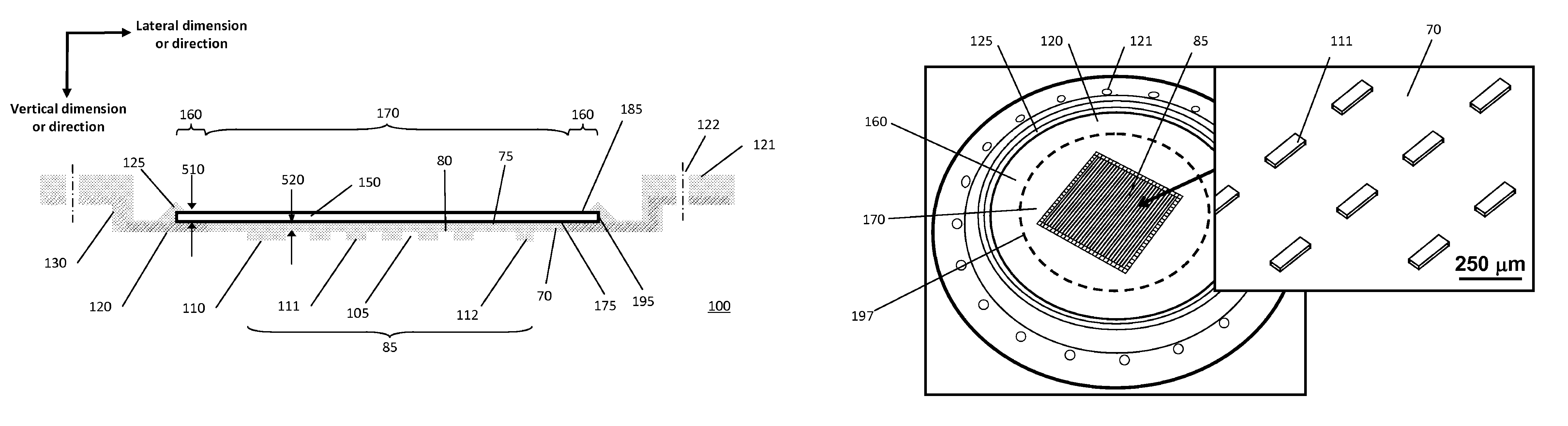
[0096]FIG. 1A provides a schematic cross-sectional view of an exemplary reinforced composite stamp 100 of the present invention. As shown in FIG. 1A, the composite stamp comprises a deformable layer 70, a reinforcement layer 120, and a rigid support layer 150. An array of relief features 105 are defined on the external surface 80 of the deformable layer 70 to facilitate selective transfer of printed structures, such as semiconductor elements. Array of relief features 105 may comprise a relief pattern providing selective printing or patterning functionality. External surface 80 is the surface of deformable layer 70 configured such that it is that is capable of contacting donor or target substrates for dry-transfer printing processes, for example providing a contact surface, printing surface or receiving surface of stamp 100 for dry transfer contact printing. The deformable layer 70 also has an internal surface 75 that faces rigid support layer 150. As shown...

example 2

Devices for Printing Using Reinforced Composite Stamps

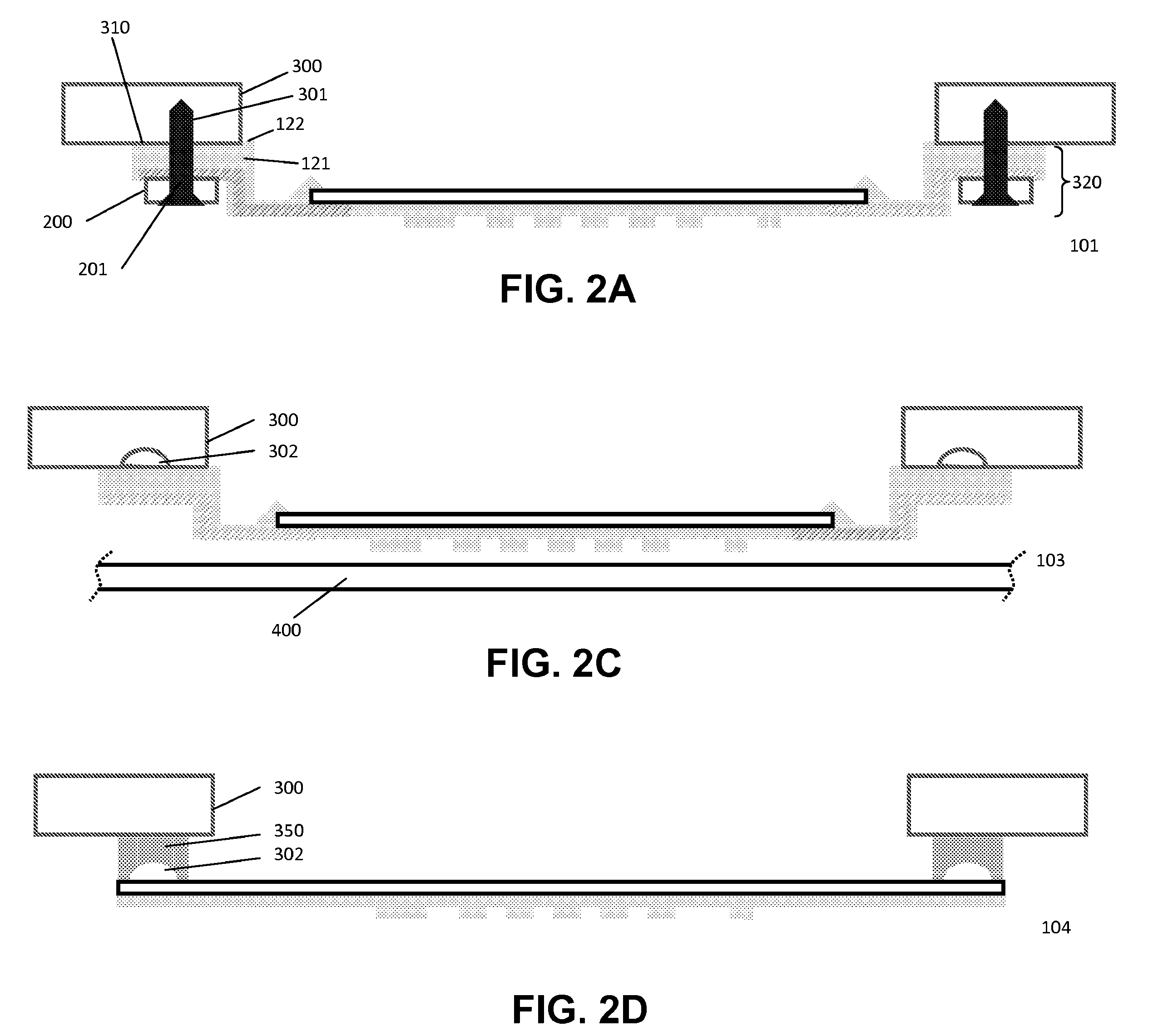
[0105]FIGS. 2A-D provides a schematic cross-sectional view of a reinforced composite stamp illustrating different examples of how a stamp of FIG. 1 is attached to a transfer printing tool head apparatus 300. Such a system can be used for a wide variety of printing methods, including dry transfer printing methods related to conformal contact with a target or a donor substrate, illustrated by 400 in FIG. 2C, where the dashed lines indicate the target or donor substrate extends and has a surface area that is larger than the printable area 85 or surface area of deformable layer 70. In each of the exemplified embodiments, the stamp and mounting design ensures there is adequate clearance distance 320 between a target substrate 400 positioned in contact with the relief features and the apparatus to which the stamp is mounted, thereby facilitating printing to a target substrate that has a surface area that is larger than the printable su...

example 3

Devices for Making Reinforced Composite Stamps

[0110]Provided herein are examples of systems and processes that can be used to make reinforced composite stamps of the present invention. FIG. 3 is a schematic illustration of a set of parts used in the process of making or molding reinforced composite stamps. One example of the steps used to make a reinforced composite stamp are as follows:

[0111]A master 402, for example a patterned master is fabricated using standard techniques, such as a UV photo-lithographic process (as described in published lithography literature; see, e.g., US Pat. Pub. No. 20060286785 to Rogers et al.). In an embodiment, master 402 is a patterned silicon wafer having relief features corresponding to the relief feature pattern desired for the deformable stamp patterned surface.

[0112]The master 402 is placed with the surface 425 having the relief feature pattern facing down in a wafer holder subassembly 403. An example wafer holder subassembly 403 is machined stai...


PUM

PropertyMeasurementUnit
thicknessaaaaaaaaaa
thicknessaaaaaaaaaa
thicknessaaaaaaaaaa

Abstract

Provided are reinforced composite stamps, devices and methods of making the reinforced composite stamps disclosed herein. Reinforced composite stamps of certain aspects of the present invention have a composition and architecture optimized for use in printing systems for dry transfer printing of semiconductor structures, and impart excellent control over relative spatial placement accuracy of the semiconductor structures being transferred. In some embodiments, for example, reinforced composite stamps of the present invention allow for precise and repeatable vertical motion of the patterned surface of the printing apparatus with self-leveling of the stamp to the surface of a contacted substrate. Reinforced composite stamps of certain aspect of the present invention achieve a uniform distribution of contact forces between the printing apparatus patterned surface and the top surface of a substrate being contacted by the reinforced composite stamp of the printing apparatus.

Description

STATEMENT REGARDING FEDERALLY SPONSORED RESEARCH OR DEVELOPMENT[0001]This invention was made, at least in part, with United States governmental support awarded by National Science Foundation Grant IIP-0712017. The United States Government has certain rights in this invention.CROSS-REFERENCE TO RELATED APPLICATIONS[0002]Not ApplicableBACKGROUND OF THE INVENTION[0003]The disclosure herein relates to the general field of systems, devices and methods for micro-and nanofabrication, including pattern transfer devices for soft lithography, contact printing, and dry transfer printing. More specifically, provided are reinforced composite stamps for printing-based assembly of semiconductor elements for the fabrication of electronic devices and systems, which provide high transfer yields and good transfer fidelity of printable semiconductor elements. In addition, processes for making and using reinforced composite stamps are disclosed.[0004]Distributed electronic systems often require large qu...

Claims


Application Information

Patent Timeline
Patent Type & Authority Patents(United States)
IPC IPC(8): H01L21/00B41L47/04B29C65/70B29C33/40B29C39/22
CPCB82Y10/00G03F7/0002B82Y40/00H01L21/0273H01L21/0274
Inventor MENARD, ETIENNE
Owner X DISPLAY CO TECH LTD
Why Eureka
Try Eureka