Light emitting device

a technology of light emitting device and pixel portion, which is applied in the direction of static indicating device, electroluminescent light source, instruments, etc., can solve the problems of inability to input video signals into the pixels at two or more rows in the pixel portion in parallel, and preferable to increase the drive frequency more than, so as to suppress the generation of pseudo contour and suppress the effect of pseudo contour

Inactive Publication Date: 2011-04-19
SEMICON ENERGY LAB CO LTD
View PDF34 Cites 11 Cited by
  • Summary
  • Abstract
  • Description
  • Claims
  • Application Information

AI Technical Summary

Benefits of technology

[0015]It is to be noted that the number of the data selecting transistors is not restricted as long as supply of drain current of one of the n driving transistors to the light emitting element can be controlled.
[0023]A Semi-amorphous semiconductor has an intermediate structure between amorphous and crystalline (including single crystalline and polycrystalline) structures. The semi-amorphous semiconductor has a third state that is stable in free energy, and has a short range order and a lattice distortion, in which crystals each having a particle size of 0.5 to 20 nm can be dispersed in a non-single crystalline semiconductor. In the semi-amorphous semiconductor, Raman spectrum is shifted to the lower frequency band than 520 cm−1 and diffraction peaks of (111) and (220) derived from a Si crystal lattice are observed by X-ray diffraction. Further, the semiconductor is mixed with at least 1 atom % of hydrogen or halogen as a neutralizing agent for dangling bond. Such a semiconductor is called herein a semi-amorphous semiconductor (SAS). A favorable semi-amorphous semiconductor with improved stability can be obtained by further promoting the lattice distortion by mixing rare gas elements such as helium, argon, krypton, and neon.
[0025]In this manner, in a light emitting device of the invention, the drive frequency of a driver circuit is suppressed while the frame frequency is increased, whereby generation of a pseudo contour can be suppressed. In addition, in a light emitting device of the invention, the drive frequency of a driver circuit is suppressed while the dividing number of a subframe period is increased, whereby generation of a pseudo contour can be suppressed.

Problems solved by technology

However, in the case of performing display using the time gray scale method, there is a problem in that a pseudo contour may be displayed in a pixel portion depending on the frame frequency.
Consequently, it is impossible to input video signals into the pixels at two or more rows in the pixel portion in parallel.
From the viewpoint of reliability of a driver circuit, however, it is not preferable to increase the drive frequency more than is necessary.

Method used


Image

  • Light emitting device
  • Light emitting device
  • Light emitting device

Examples


embodiment 1

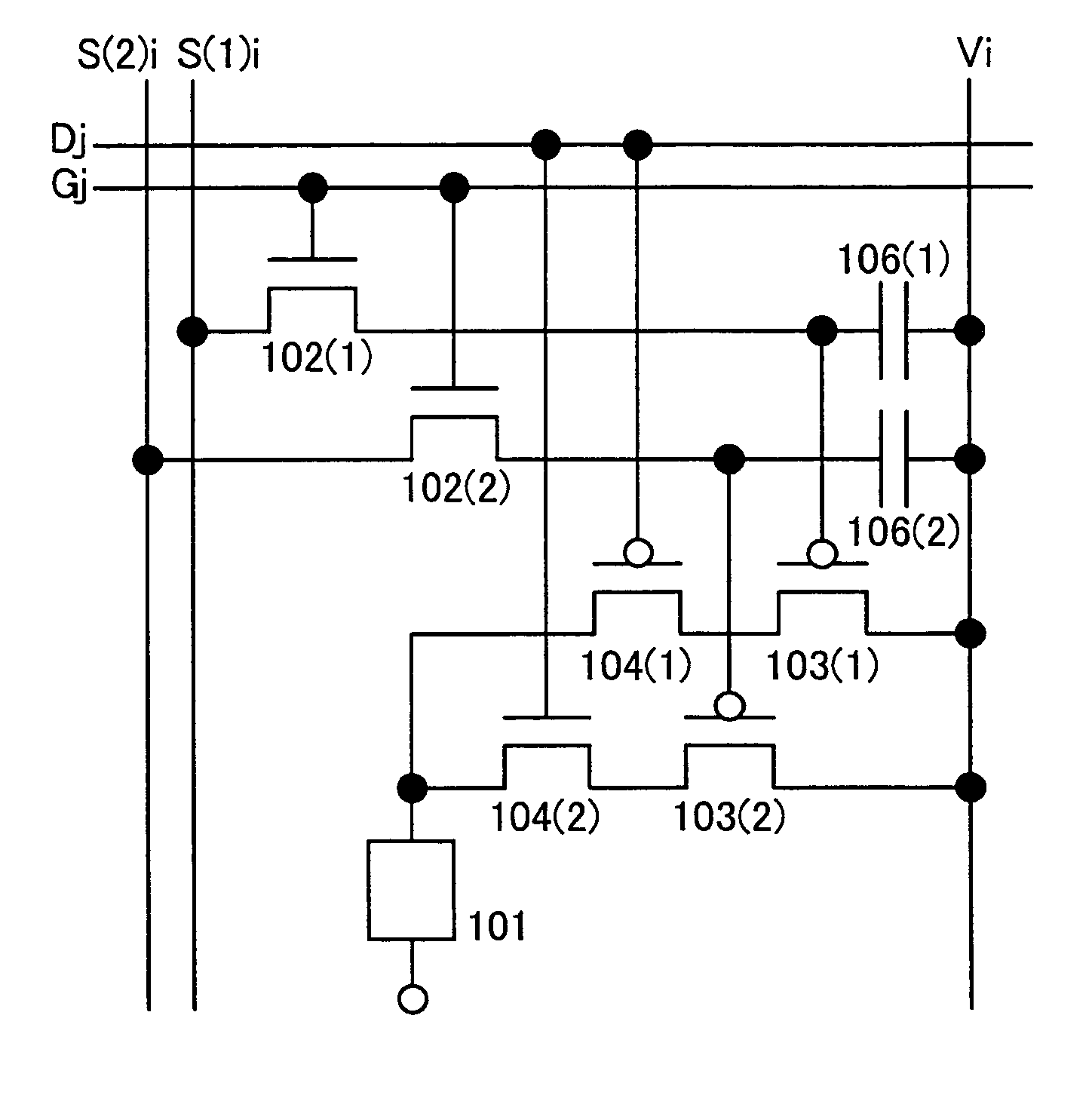
[0100]In this embodiment, a layout of a pixel in a light emitting device of the invention is described. Note that in this embodiment, a pixel in FIG. 1 where the first capacitor 106(1) and the second capacitor 106(2) are not provided is described as an example.

[0101]A top view of the pixel shown in FIG. 1 is illustrated in FIG. 9. In FIG. 9, the scan line Gj partially functions as a gate 903 of the first switching transistor 102(1) and a gate 904 of the second switching transistor 102(2).

[0102]In addition, the first driving transistor 103(1) and the first data selecting transistor 104(1) share an active layer 905 while the second driving transistor 103(2) and the second data selecting transistor 104(2) share an active layer 906 in FIG. 9.

[0103]The selecting line Dj partially functions as a gate 907 of the first data selecting transistor 104(1) and a gate 908 of the second data selecting transistor 104(2) in FIG. 9.

[0104]Note that as for the light emitting element 101, a first electr...

embodiment 2

[0105]In this embodiment, driver circuits employed in the light emitting device of the invention are described. FIG. 10 is a block diagram of a light emitting device in this embodiment. The light emitting device shown in FIG. 10 comprises a pixel portion 1111 including a plurality of pixels each having a light emitting element, a scan line driver circuit 1112 for selecting each the pixel, a signal line driver circuit 1113 for controlling input of a video signal into the selected pixel, and a selecting line driver circuit 1120 for controlling potential of a selecting line.

[0106]In FIG. 10, the signal line driver circuit 1113 includes a shift register 1114, a latch A 1115, and a latch B 1116. A clock signal (SCLK), a start pulse signal (SSP), and a switching-over signal (L / R) are inputted into the shift register 1114. When the clock signal (SCLK) and the start pulse signal (SSP) are inputted, a timing signal is generated in the shift register 1114. According to the switching-over sign...

embodiment 3

[0115]In this embodiment, a cross-sectional structure of a pixel where a driving transistor is a P-channel type is described using FIGS. 11A to 11C. Note that a first electrode is an anode while a second electrode is a cathode in FIGS. 11A to 11C, however, it is possible that the first electrode is a cathode while the second electrode is an anode as well.

[0116]FIG. 11A is a cross-sectional view of a pixel where a driving transistor 6001 and a data selecting transistor 6002 are P-channel types and light emitted from a light emitting element 6003 is extracted from a first electrode 6004 side. Although the first electrode 6004 of the light emitting element 6003 is electrically connected to the data selecting transistor 6002 in FIG. 11A, the first electrode 6004 of the light emitting element 6003 may be electrically connected to the driving transistor 6001.

[0117]The driving transistor 6001 and the data selecting transistor 6002 are covered with an interlayer insulating film 6007, and a ...


PUM


Abstract

A light emitting device with generation of a pseudo contour suppressed is provided in which the drive frequency of a driver circuit is suppressed while the frame frequency is increased. In addition, a light emitting device with generation of a pseudo contour suppressed is provided in which the drive frequency of a driver circuit is suppressed while the dividing number of a subframe period is increased. To input plural bits of video signals into pixels in parallel, a switching transistor and a driving transistor are provided in each pixel in accordance with the number of the bits. In addition, a transistor for selecting a video signal (a data selecting transistor) is provided in each pixel in order to select each bit of a video signal within the pixel when display is actually performed at the pixels.

Description

BACKGROUND OF THE INVENTION[0001]1. Field of the Invention[0002]The present invention relates to a light emitting device in which a plurality of pixels each comprises a light emitting element and a means for supplying current to the light emitting element.[0003]2. Description of the Related Art[0004]As a driving method of a light emitting device, there is a time gray scale method in which a gray scale is displayed by controlling a light emitting period of a pixel in one frame period by use of binary voltage of a digital video signal. Electroluminescent materials are more suitable for a time gray scale method than liquid crystals and the like since the response speed is generally faster. Specifically, when displaying by the time gray scale method, one frame period is divided into a plurality of subframe periods. Then, a pixel emits light or does not emit light according to a video signal in each of the subframe periods. According to the aforementioned structure, the total actual ligh...

Claims


Application Information

Patent Timeline
Patent Type & Authority Patents(United States)
IPC IPC(8): G09G3/32G09G3/28H05B44/00
CPCG09G3/2022G09G3/3208G09G2320/0266G09G2310/0262G09G2320/0261G09G2300/0809
Inventor OZAKI, TADAFUMI
Owner SEMICON ENERGY LAB CO LTD
Why Eureka
Try Eureka