Package structure fabrication method

Active Publication Date: 2011-05-03
SILICONWARE PRECISION IND CO LTD
32 Cites 152 Cited by

AI-Extracted Technical Summary

Problems solved by technology

However, with the metal plate 10 being unfit for routing, lengthy bonding wires are required, thereby increasing the cost and adversely affecting the electrical performance of the package.
However, the above-described technique incurs high costs and requires complicated processes and is not suitable for mass production because of the necessity of forming the dielectric layer 100 on the metal plate 10 and forming the wiring layer 11′ b...

Method used

[0040]In the present embodiment, the first encapsulant 24a is formed to cover the die pad 210 and the wiring layers 21 so as to provide an even surface. As such, when the chip 22 is disposed above the first encapsulant 24a, cracks will not occur to the first encapsulant 24a, thereby preventing the conventional drawbacks caused by the use of a solder mask layer and greatly improving the product quality.
[0041]Further, the present invention dispenses with a solder mask layer for covering the die pad 210 and the wiring layers 21 and accordingly does not require a lithography process for forming openings in a solder mask layer,...

Benefits of technology

[0022]According to the present invention, the first encapsulant is formed to cover the wiring layer so as to provide an even surface. As such, when the chip is disposed on the first encapsulant, cracks will not occur to the first encapsulant, thereby preventing the conventional drawbacks caused by the use of a sol...

Abstract

A fabrication method of a package structure includes: preparing a metal plate having first and second surfaces and defined with an active region; forming a wiring layer with conductive traces and first electrical contact pads on the first surface; forming third electrical contact pads corresponding to the first electrical contact pads on the second surface; forming a first encapsulant on the first surface; forming on the second surface an open area to penetrate the metal plate, wherein the metal plate form conductive posts between the first and third electrical contact pads; mounting in the open area a chip electrically connected to the wiring layer; forming a second encapsulant in the open area, the wiring layer and the third electrical contact pads; forming first and second openings in the first and second encapsulants to expose the third electrical contact pads, respectively; and cutting the metal plate to remove the metal layer.

Application Domain

Technology Topic

Image

  • Package structure fabrication method
  • Package structure fabrication method
  • Package structure fabrication method

Examples

  • Experimental program(2)

Example

First Embodiment
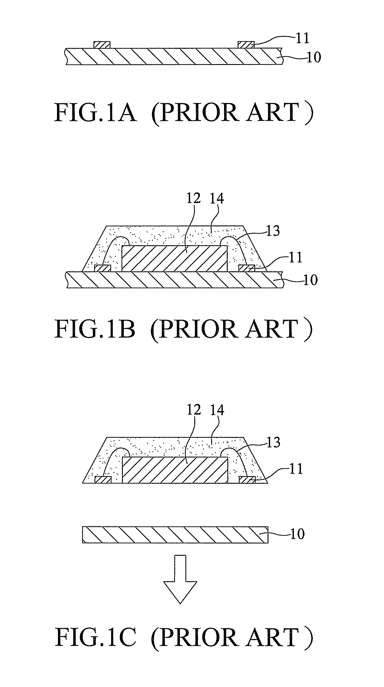
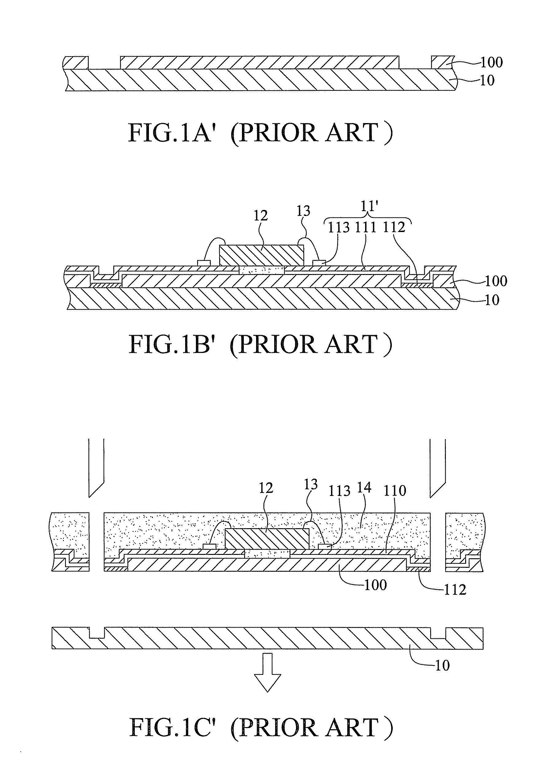
[0030]FIGS. 2A to 2H are schematic views showing a fabrication method of a package structure according to a first embodiment of the present invention. For the purpose of brevity, only one package unit is shown in the drawings. But it should be noted that the present invention is not limited thereto. For example, a plurality of package units arranged in array are provided in practice
[0031]Referring to FIG. 2A, a metal plate 20 having a first surface 20a and an opposed second surface 20b is provided, and at least an active region A is defined on the metal plate 20. Then, a resist layer 200 such as photo resist is formed on the first and second surfaces 20a, 20b, and a plurality of patterned open areas 200a is formed in the resist layer 200 for exposing portions of the first and second surfaces 20a, 20b of the metal plate 20. Further, a patterned metal layer 201 is formed in the open areas 200a by electroplating, wherein the metal layer 201 on the first surface 20a inside the active region A comprises a die pad 210 and a plurality of wiring layers 21. The metal layer 201 on the first and second surfaces 20a, 20b outside the active region A serve as an anti-etching structure 214 in a subsequent etching process.
[0032]In the present embodiment, the metal plate 20 is made of copper, and the die pad 210 and the wiring layers 21 are made of at least one selected from the group consisting of gold, palladium, and nickel. The wiring layers 21 each have a plurality of conductive traces 211, a plurality of first electrical contact pads 212 and bond fingers 213 formed at two ends of the conductive traces 211, respectively, wherein the first electrical contact pad 212 serve as ball pads, as shown in FIG. 2B′.
[0033]Referring to FIG. 2B, there is shown a sectional view of FIG. 2B′, the resist layer 200 is removed to expose portions of the first surface 20a and the second surface 20b in the active region A. Referring to FIG. 2B′, the wiring layers 21 are located at the periphery of the die pad 210.
[0034]Referring to FIG. 2C, a first encapsulant 24a is formed on the first surface 20a to extend beyond the active region A to cover the die pad 210 and the wiring layers 21, thereby embedding the die pad 210 and the wiring layers 21 in the first encapsulant 24a. The first encapsulant 24a is of a thickness substantially between 0.1 and 0.5 mm, and is made of an epoxy resin polymer material such as EMC (epoxy mold compound), PP (prepeg), ABF (Ajinomoto build-up film) and the like.
[0035]Referring to FIG. 2D, the metal plate 20 is etched from the second surface 20b in the active region A along the edges of the anti-etching structure 214 so as to form an open area 202 penetrating the metal plate 20, and in consequence the die pad 210 and the wiring layers 21 are exposed from the open area 202.
[0036]Referring to FIG. 2E, a chip 22 is disposed on the die pad 210 in the open area 202 and electrically connected to the bond fingers 213 of the wiring layers 21 through a plurality of bonding wires 23.
[0037]Referring to FIG. 2F, a second encapsulant 24b is formed on the metal plate 20 in the open area 202 to cover the chip 22, the wiring layers 21 and the bonding wires 23 and extend beyond the open area 202. The second encaspulant 24b is made of the same material as the first encapsulant 24a, for example, EMC.
[0038]Referring to FIG. 2G, a plurality of openings 240 is formed in the first encapsulant 24a by drilling such that the first electrical contact pads 212 are exposed from the openings 240, wherein the first electrical contact pads 212 are of a width of about 20 μm greater than the diameter of the openings 240. Portions of the die pad 210 are selectively exposed from the openings 240 to serve as second electrical contact pads 215. Conductive elements 25, such as solder balls or conductive bumps, are formed on the first and second electrical contact pads 212, 215 such that a printed circuit board can be mounted on the conductive elements 25.
[0039]Referring to FIG. 2H, the metal plate 20 is cut and removed so as to form a package structure 2.
[0040]In the present embodiment, the first encapsulant 24a is formed to cover the die pad 210 and the wiring layers 21 so as to provide an even surface. As such, when the chip 22 is disposed above the first encapsulant 24a, cracks will not occur to the first encapsulant 24a, thereby preventing the conventional drawbacks caused by the use of a solder mask layer and greatly improving the product quality.
[0041]Further, the present invention dispenses with a solder mask layer for covering the die pad 210 and the wiring layers 21 and accordingly does not require a lithography process for forming openings in a solder mask layer, thus reducing the cost and facilitating mass production.

Example

Second Embodiment
[0042]FIGS. 3A to 3F are sectional views showing a fabrication method of a package structure according to a second embodiment of the present invention. The second embodiment differs from the first embodiment in that the conductive posts 36 in the second embodiment are formed for facilitating a stacking process.
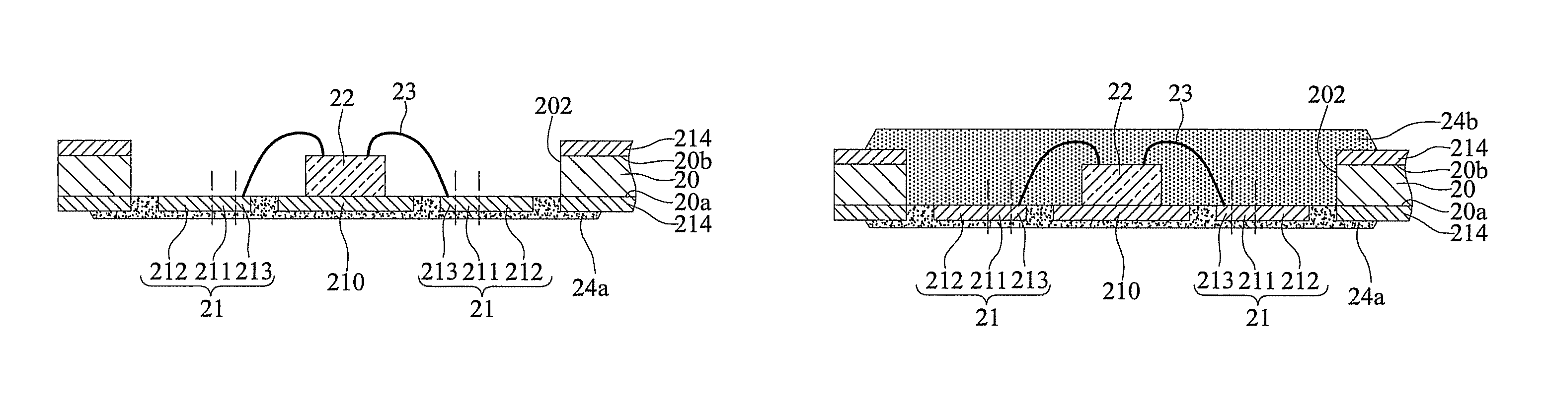
[0043]Referring to FIG. 3A, a metal plate 30 with a structure as shown in FIG. 2C is provided, and a plurality of third electrical contact pads 301 corresponding in position to the first electrical contact pads 312 is formed on the second surface 30b in the active region A.
[0044]Referring to FIG. 3B, the metal plate 30 is etched from the second surface 30b in the active region A along the inner edges of an anti-etching structure 314 and edges of the third electrical contact pads 301 so as to form an open area 302 to penetrate the metal plate 30, and in consequence the die pad 310, wiring layers 311 and bond fingers 313 are exposed from the open area 302. Therein, the portions of the metal plate 30 located between the first electrical contact pads 312 and the third electrical contact pads 301 corresponding in position thereto are shielded by the third electrical contact pads 301 and thus not etched away during the etching process to thereby form a plurality of conductive posts 36
[0045]Referring to FIG. 3C, a chip 32 is mounted on the die pad 310 and electrically connected to the bond fingers 313 through a plurality of bonding wires 33; further, a second encapsulant 34b is formed in the open area 302 to cover the chip 32, the conductive posts 36, the wiring layers 31, and the bonding wires 33.
[0046]Referring to FIG. 3D, a plurality of first openings 340a is formed in the first encapsulant 34a by laser drilling for exposing the first electrical contact pads 312 and the second electrical contact pads 315. As such, conductive elements 35 can further be formed on the first and second electrical contact pads 312, 315 to allow a printed circuit board to be mounted on the conductive elements 35; meanwhile, a plurality of second openings 340b is formed in the second encaspulant 34b for exposing portions of the third electrical contact pads 301 on the conductive posts 36.
[0047]Referring to FIG. 3E, the metal plate 30 is cut and removed to form a package structure 3.
[0048]Referring to FIG. 3F, another package structure 3′ is stacked on the conductive posts 36 via the conductive elements 35′ thereof.
[0049]According to the present invention, the first encapsulant is formed to cover the wiring layers so as to provide an even surface thereof. As such, when the chip is disposed on the first encapsulant, cracks will not occur to the first encapsulant, thereby greatly improving the product quality.
[0050]Further, the present invention dispenses with a solder mask layer for covering the die pad and the wiring layers and accordingly does not require a lithography process for forming openings in a solder mask layer, thus reducing the cost and facilitating mass production.
[0051]The above-described descriptions of the specific embodiments are intended to illustrate the preferred implementation according to the present invention but are not intended to limit the scope of the present invention. Accordingly, all modifications and variations completed by those with ordinary skill in the art should fall within the scope of present invention defined by the appended claims.

PUM

PropertyMeasurementUnit
Electrical conductor
Area
tensileMPa
Particle sizePa
strength10

Description & Claims & Application Information

We can also present the details of the Description, Claims and Application information to help users get a comprehensive understanding of the technical details of the patent, such as background art, summary of invention, brief description of drawings, description of embodiments, and other original content. On the other hand, users can also determine the specific scope of protection of the technology through the list of claims; as well as understand the changes in the life cycle of the technology with the presentation of the patent timeline. Login to view more.

Similar technology patents

Classification and recommendation of technical efficacy words

Why Eureka
Try Eureka